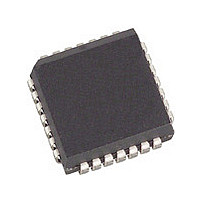
PBL386202QNAXT Infineon Technologies, PBL386202QNAXT Datasheet - Page 42

PBL386202QNAXT
Manufacturer Part Number
PBL386202QNAXT
Description
Manufacturer
Infineon Technologies
Datasheet
1.PBL386202QNAXT.pdf
(46 pages)
Specifications of PBL386202QNAXT
Number Of Channels
1
On-hook Transmission
Yes
Polarity Reversal
Yes
On-chip Ring Relay Driver
Yes
Operating Temp Range
0C to 70C
Package Type
PLCC
Loop Current Limit
30mA
Operating Temperature Classification
Commercial
Pin Count
28
Mounting
Surface Mount
Operating Supply Voltage (max)
5.25/-58V
Lead Free Status / RoHS Status
Compliant
voltage (that is the battery voltage,
supply voltage the overvoltage stress on the SLIC is minimized.
Positive overvoltages are clamped to ground by a diode. Negative overvoltages are
initially clamped close to the SLIC negative supply rail voltage and the protector will
crowbar into a low voltage on-state condition, by firing an internal thyristor.
A gate decoupling capacitor,
enough current to quickly turn on the thyristor in the protector.
close to the overvoltage protection device. Without the capacitor even the low
inductance in the track to the
the thyristor clamp.
The fuse resistors
dissipators when transients are clamped, and of being fuses when the line is exposed to
a power cross. If a PTC is choosen for
in series with resistors not sensitive to temperature, as the PTC will act as a capacitance
for fast transients and therefore will not protect the SLIC.
11
No special power-up sequence is necessary, except that ground has to be present
before all other power supply voltages.
12
Care in Printed Circuit Board (PCB) layout is essential for proper function. The
components connected to the RSN input should be placed in close proximity to that pin,
such that no interference is injected into the receive summing node (RSN). Ground plane
surrounding the RSN pin is advisable.
Analog Ground (AGND) should be connected to Battery Ground (BGND) on the PCB, in
one point. The capacitors for the battery should be connected with short wide leads of
the same length.
Data Sheet
Power-Up Sequence
Printed Circuit Board Layout
R
F
serve the dual purposes of being non-destructive energy
C
V
B
GG
supply will limit the current and delay the activation of
, is needed to carry enough charge to supply a high
V
B
). As the protection voltage will track the negative
R
F
, note that it is important to always use PTC’s
42
C
Power-Up Sequence
GG
Rev. 2.0, 2005-04-13
should be placed
PBL 38620/2
FlexiSLIC


