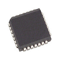
PBL386202QNAXT Infineon Technologies, PBL386202QNAXT Datasheet - Page 40

PBL386202QNAXT
Manufacturer Part Number
PBL386202QNAXT
Description
Manufacturer
Infineon Technologies
Datasheet
1.PBL386202QNAXT.pdf
(46 pages)
Specifications of PBL386202QNAXT
Number Of Channels
1
On-hook Transmission
Yes
Polarity Reversal
Yes
On-chip Ring Relay Driver
Yes
Operating Temp Range
0C to 70C
Package Type
PLCC
Loop Current Limit
30mA
Operating Temperature Classification
Commercial
Pin Count
28
Mounting
Surface Mount
Operating Supply Voltage (max)
5.25/-58V
Lead Free Status / RoHS Status
Compliant
7.3
Ring trip detection is accomplished by connecting an external network to a comparator
in the SLIC with inputs DT and DR. The ringing source can be balanced or unbalanced
superimposed on
the ring lead or the tip lead with return via the other wire. A ring relay driven by the SLIC
ring relay driver connects the ringing source to tip and ring.
The ring trip function is based on a polarity change at the comparator input when the line
goes off-hook. In the on-hook state no DC current flows through the loop and the voltage
at comparator input DT is more positive than the voltage at input DR. When the line goes
off-hook, while the ring relay is energized, DC current flows and the comparator input
voltage reverses polarity.
Figure 8
when the ring voltage is superimposed on
wire port. The DC voltage across sense resistor
comparator input DT and DR via the network
When the line is on-hook (no DC current), DT is more positive than DR and the DET
output will report logic level high, that is the detector is not tripped. When the line goes
off-hook, while ringing, a DC current will flow through the loop including sense resistor
R
output DET to logic level low, that is tripped detector conditions. The system controller
(or line card processor) responds by de-energizing the ring relay, that is ring trip.
Complete filtering of the 20 Hz AC component at terminal DT and DR is not necessary.
A toggling DET output can be examined by a software routine to determine the duty
cycle. When the DET output is at logic level low for more than half the time, off-hook
conditions is indicated.
8
The PBL 38620/2 SLIC incorporates a ring relay driver designed as open collector (npn),
with a current sinking capability of 50 mA. The drive transistor emitter is connected to
BGND. The relay driver has an internal zener diode clamp for inductive kick back
voltages.
Data Sheet
RT
and will cause input DT to become more negative than input DR. This changes
gives an example of a ring trip detector network. This network is applicable
Ring Trip Detector
Relay Driver
V
B
or GND. The unbalanced ringing source may be applied to either
V
40
B
and is injected on the ring lead of the two-
R
1
,
R
2
,
R
R
3
RT
,
R
is monitored by the ring trip
4
,
C
1
and
C
Rev. 2.0, 2005-04-13
2
.
PBL 38620/2
Relay Driver
FlexiSLIC


