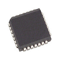
PBL386202QNAXT Infineon Technologies, PBL386202QNAXT Datasheet - Page 41

PBL386202QNAXT
Manufacturer Part Number
PBL386202QNAXT
Description
Manufacturer
Infineon Technologies
Datasheet
1.PBL386202QNAXT.pdf
(46 pages)
Specifications of PBL386202QNAXT
Number Of Channels
1
On-hook Transmission
Yes
Polarity Reversal
Yes
On-chip Ring Relay Driver
Yes
Operating Temp Range
0C to 70C
Package Type
PLCC
Loop Current Limit
30mA
Operating Temperature Classification
Commercial
Pin Count
28
Mounting
Surface Mount
Operating Supply Voltage (max)
5.25/-58V
Lead Free Status / RoHS Status
Compliant
9
The SLIC has three digital control inputs, C1, C2 and C3 (see
SLIC interprets the control input condition and sets up the commanded operating state.
C1, C2 and C3 are internally pulled up.
9.1
In the Open Circuit state, the TIPX and RINGX line drive amplifiers as well as other circuit
blocks are powered down. This causes the SLIC to present a high impedance to the line.
Power dissipation is at a minimum and no detectors are active. DET output is set high.
9.2
The ring relay driver and the ring trip detector are activated and the ring trip detector is
indicating off-hook with a logic low level at the detector output.
As the SLIC does not have any stand by state the SLIC will remain in the active normal
state.
9.3
TIPX is the terminal closest to ground and sources loop current while RINGX is the more
negative terminal and sinks loop current. VF signal transmission is normal. The loop
current detector or ground key detector is activated. The loop current detector indicates
off-hook with a logic low level and the ground key detector is indicating active ground key
with a logic high level present at the detector output.
10
10.1
The SLIC must be protected against foreign voltages on the telephone line.
Overvoltages can result from lightning, AC power contact, induction and other causes.
Refer to
voltages that may be applied to the SLIC.
10.2
The circuit shown in
programmable overvoltage protector (OVP, for example Bournes TISP PBL2) as
secondary protection.
The TISP PBL2 is a dual forward-conducting buffered p-gate overvoltage protector. The
protector gate references the protection (clamping) voltage to the negative supply
Data Sheet
Table
Control Inputs
Open Circuit (C3, C2, C1 = 0, 0, 0)
Ringing (C3, C2, C1 = 0, 0, 1)
Active states
Overvoltage Protection
Overvoltage Protection - General
Secondary Protection
3, TIPX and RINGX terminals, for maximum continuous and transient
Figure 8
utilizes series resistors (
41
R
Table
F1
,
R
F2
2). A decoder in the
Rev. 2.0, 2005-04-13
) together with a
Control Inputs
PBL 38620/2
FlexiSLIC


