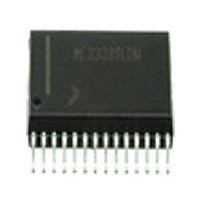
MC33889BDW Freescale, MC33889BDW Datasheet - Page 48

MC33889BDW
Manufacturer Part Number
MC33889BDW
Description
Manufacturer
Freescale
Datasheet
1.MC33889BDW.pdf
(60 pages)
Specifications of MC33889BDW
Number Of Transceivers
1
Standard Supported
CAN 2.0
Operating Supply Voltage (max)
18V
Operating Supply Voltage (min)
5.5V
Package Type
SOIC W
Supply Current
45mA
Operating Temperature (max)
125C
Operating Temperature (min)
-40C
Operating Temperature Classification
Automotive
Mounting
Surface Mount
Pin Count
28
Lead Free Status / RoHS Status
Not Compliant
Available stocks
Company
Part Number
Manufacturer
Quantity
Price
Company:
Part Number:
MC33889BDW
Manufacturer:
FREESCALE Semiconductor
Quantity:
26
Part Number:
MC33889BDW
Manufacturer:
FREESCALE
Quantity:
20 000
Table 24. Status bits
TIM REGISTERS
TIM REGISTER
Table 25. TIM Register.
48
33889
FUNCTIONAL DEVICE OPERATION
LOGIC COMMANDS AND REGISTERS
Description: This register is split into 2 sub registers, TIM1 and TIM2.
TIM1 controls the watchdog timing selection as well as the window or timeout option. TIM1 is selected when bit D3 is 0.
TIM2 is used to define the timing for the cyclic sense and forced wake-up function. TIM2 is selected when bit D3 is 1.
No read operation is allowed for registers TIM1 and TIM2
L0WUb
Reset condition
L1WUb
0
1
0
0
1
$101b
Reset
TIM1
L0WUa
0
1
1
L1WUa
0
1
W
R
FDIS bit in CAN
register
0
0
1
D3
0
Wake-up occurred at L0 (sleep or stop mode with L0 filter disable). WUR must be set
No wake-up occurred at L1 (sleep or stop mode).
High level state on L1 (standby or normal mode)
Low level state on L1 (standby or normal mode)
Wake-up occurred at L1 (sleep or stop mode).
POR, RESET
WDW
No wake-up occurred at L0 (sleep or stop mode).
High level state on L0 (standby or normal mode)
Low level state on L0 (standby or normal mode)
D2
Wake-up occurred at L0 (sleep or stop mode).
0
to xx00 before sleep or stop mode.
Description
Description
POR, RESET
WDT1
Analog Integrated Circuit Device Data
D1
0
Freescale Semiconductor
POR, RESET
WDT0
D0
0


