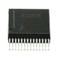
MC33889BDW Freescale, MC33889BDW Datasheet - Page 40

MC33889BDW
Manufacturer Part Number
MC33889BDW
Description
Manufacturer
Freescale
Datasheet
1.MC33889BDW.pdf
(60 pages)
Specifications of MC33889BDW
Number Of Transceivers
1
Standard Supported
CAN 2.0
Operating Supply Voltage (max)
18V
Operating Supply Voltage (min)
5.5V
Package Type
SOIC W
Supply Current
45mA
Operating Temperature (max)
125C
Operating Temperature (min)
-40C
Operating Temperature Classification
Automotive
Mounting
Surface Mount
Pin Count
28
Lead Free Status / RoHS Status
Not Compliant
Available stocks
Company
Part Number
Manufacturer
Quantity
Price
Company:
Part Number:
MC33889BDW
Manufacturer:
FREESCALE Semiconductor
Quantity:
26
Part Number:
MC33889BDW
Manufacturer:
FREESCALE
Quantity:
20 000
are data send from MCU to SBC or read back from SBC to MCU.
to be set at the “reset value”.
40
33889
FUNCTIONAL DEVICE OPERATION
LOGIC COMMANDS AND REGISTERS
The SPI is a 8 bit SPI. First 3 bits are used to identify the internal SBC register address, bit 4 is a read/write bit. The last 4 bits
During write operation state of MISO has no signification.
During read operation only the last 4 bits at MISO have a meaning (content of the accessed register)
Following tables describe the SPI register list, and register bit meaning.
Registers “reset value” is also described, as well as the “reset condition”. reset condition is the condition which cause the bit
Possible reset condition are:
Power On Reset: POR
SBC mode transition:
NR2R - Normal Request to Reset mode
NR2N - Normal Request to Normal mode
N2R - Normal to Reset mode
STB2R - Standby to Reset mode
STO2R - Stop to Reset mode
SBC mode:RESET - SBC in Reset mode
MISO
Bit7
A2
Bit6
A1
address
Bit5
A0
R/W
Bit4
LOGIC COMMANDS AND REGISTERS
Figure 20. Data Format Description
Bit3
D3
SPI INTERFACE
Bit2
D2
data
Bit1
D1
Bit0
D0
MOSI
Analog Integrated Circuit Device Data
Read operation: R/W bit = 0
Write operation: R/W bit = 1
Freescale Semiconductor


