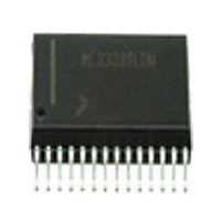
MC33889BDW Freescale, MC33889BDW Datasheet - Page 26

MC33889BDW
Manufacturer Part Number
MC33889BDW
Description
Manufacturer
Freescale
Datasheet
1.MC33889BDW.pdf
(60 pages)
Specifications of MC33889BDW
Number Of Transceivers
1
Standard Supported
CAN 2.0
Operating Supply Voltage (max)
18V
Operating Supply Voltage (min)
5.5V
Package Type
SOIC W
Supply Current
45mA
Operating Temperature (max)
125C
Operating Temperature (min)
-40C
Operating Temperature Classification
Automotive
Mounting
Surface Mount
Pin Count
28
Lead Free Status / RoHS Status
Not Compliant
Available stocks
Company
Part Number
Manufacturer
Quantity
Price
Company:
Part Number:
MC33889BDW
Manufacturer:
FREESCALE Semiconductor
Quantity:
26
Part Number:
MC33889BDW
Manufacturer:
FREESCALE
Quantity:
20 000
INTRODUCTION
sleep and stop modes. All modes are controlled by the SPI.
An additional temporary mode called “normal request mode”
is automatically accessed by the device (refer to state
machine) after wake-up events. Special mode and
configurations are possible for software application debug
and flash memory programming.
NORMAL MODE
to the normal application operation. All functions are
available in this mode (watchdog, wake-up input reading
through the SPI, HS1 activation, and CAN communication).
The software watchdog is running and must be periodically
cleared through the SPI.
STANDBY MODE
disabling the V2CTRL pin. The CAN cell is not available, as
powered from V2. Other functions are available: wake-up
input reading through the SPI and HS1 activation. The
watchdog is running.
SLEEP MODE
powered. The device can be awakened internally by cyclic
sense via the wake-up input pins and HS1 output, from the
forced wake function, the CAN physical interface, and the SPI
(CS pin).
STOP MODE
Regulator 1 is activated in a special low power mode which
allows it to deliver 2.0 mA. The objective is to supply the MCU
of the application while it is turned into a power saving
condition (i.e stop or wait mode).
dedicated to powering the Microcontroller when it is in low
power mode (stop, pseudo stop, wait etc.). In these modes,
the MCU supply current is less than 1.0 mA. The MCU can
restart its software application very quickly without the
complete power up and reset sequence.
SBC), the application can wake-up from the SBC side (ex
cyclic sense, forced wake-up, CAN message, wake-up
inputs) or the MCU side (key wake-up etc.).
becomes active 20
26
33889
FUNCTIONAL DEVICE OPERATION
OPERATIONAL MODES
The device has four modes of operation, normal, stand-by,
In this mode both regulators are ON, and this corresponds
Only the Regulator 1 is ON. Regulator 2 is turned OFF by
Regulators 1 and 2 are OFF. In this mode, the MCU is not
Regulator 2 is turned OFF by disabling the V2CTRL pin.
Stop mode is entered through the SPI. Stop mode is
When the application is in stop mode (both MCU and
When Stop mode is selected by the SPI, stop mode
µ
s after end of the SPI message. The “go
FUNCTIONAL DEVICE OPERATION
OPERATIONAL MODES
to stop” instruction must be the last instruction executed by
the MCU before going to low power mode.
“not running” depending on the selection by the SPI. Refer to
the SPI description, RCR register bit WDSTOP. If the W/D is
enabled, the SBC must wake-up before the W/D time has
expired, otherwise a reset is generated. In stop mode, the
SBC wake-up capability is identical as in sleep mode.
STOP MODE: WAKE-UP FROM SBC SIDE, INT PIN
ACTIVATION
the SBC side. When a wake-up is detected by the SBC (CAN,
Wake-up input, forced wake-up, etc.), the SBC turns itself
into Normal request mode and activates the VDD1 main
regulator. When the main regulator is fully active, then the
wake-up is signalled to the MCU through the INT pin. The INT
pin is pulled low for 10
events can be read through the SPI registers.
STOP MODE: WAKE-UP FROM MCU SIDE
may come to the MCU. In this case, the MCU has to signal to
the SBC that it has to go into Normal mode in order for the
VDD1 regulator to be able to deliver full current capability.
This is done by a low to high transition of the CS pin. The CS
pin low to high activation has to be done as soon as possible
after the MCU. The SBC generates a pulse at the INT pin.
Alternatively the L0 and L1 inputs can also be used as wake-
up from the Stop mode.
STOP MODE CURRENT MONITORING
threshold, the SBC jumps into Normal request mode,
activates the VDD1 main regulator, and generates an
interrupt to the MCU. This interrupt is not maskable and a not
bit are set into the INT register.
SOFTWARE WATCHDOG IN STOP MODE
set), the MCU has to wake-up independently of the SBC
before the end of the SBC watchdog time. In order to do this,
the MCU has to signal the wake-up to the SBC through the
SPI wake-up (CS pin low to high transition to activated the
SPI wake-up). Then the SBC wakes up and jumps into the
normal request mode. The MCU has to configure the SBC to
go to either into normal or standby mode. The MCU can then
choose to go back into stop mode.
SBC will activate the reset pin and jump into the normal
request mode. The MCU can then be initialized.
In Stop mode, the Software watchdog can be “running” or
When an application is in stop mode, it can wake-up from
When the application is in stop mode, the wake-up event
If the current in Stop mode exceeds the I
If the watchdog is enabled (register MCR, bit WDSTOP
If no MCU wake-up occurs within the watchdog timing, the
Analog Integrated Circuit Device Data
µ
s and then returns high. Wake-up
Freescale Semiconductor
DD1S-WU


