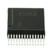
MC33742SDW Freescale, MC33742SDW Datasheet - Page 58

MC33742SDW
Manufacturer Part Number
MC33742SDW
Description
Manufacturer
Freescale
Datasheet
1.MC33742SDW.pdf
(70 pages)
Specifications of MC33742SDW
Data Rate
1000Kbps
Number Of Transceivers
1
Standard Supported
CAN 2.0
Operating Supply Voltage (max)
27V
Operating Supply Voltage (typ)
5/9/12/15/18/24V
Operating Supply Voltage (min)
4.5V
Package Type
SOIC W
Supply Current
45mA
Operating Temperature (max)
125C
Operating Temperature (min)
-40C
Operating Temperature Classification
Automotive
Mounting
Surface Mount
Pin Count
28
Lead Free Status / RoHS Status
Not Compliant
Available stocks
Company
Part Number
Manufacturer
Quantity
Price
Part Number:
MC33742SDW
Manufacturer:
MOTOROLA/摩托罗拉
Quantity:
20 000
VOLTAGE REGULATOR
fully integrated and protected, and a V2 regulator, which
operates with an external ballast transistor.
VDD REGULATOR
with current capability of 200mA max. It requires external
decoupling and stabilizing capacitors. The minimum
recommended values are as follows:
• C4: 100nF
• C3: 10μF < C3 <22μF, ESR < 1.0Ω or
• C3: 22μF < C3 <47μF, ESR < 5.0Ω or
• C3: ≥ 47μF, ESR < 10Ω
V2 REGULATOR: OPERATING WITH EXTERNAL
BALLAST TRANSISTOR
Its accuracy relative to VDD is ±1.0%. It requires external
decoupling and stabilizing capacitors.
FAILURE ON VDD, WDOG, RESET, AND INT PINS
and of the INT, RST, and WDOG pins at power-up and under
failure of the VDD regulator.
POWER-UP AND SBC ENTERING NORMAL
OPERATION
(CAN interface is in TXRX mode): VDD is on and V2 is off.
58
33742
TYPICAL APPLICATIONS
The SBC contains two 5.0V regulators: a V1 regulator,
The VDD regulator provides 5.0V output, 2.0% accuracy
The V2 regulator is a tracking regulator of the VDD output.
The paragraphs below describe the behavior of the device
After power-up the 33742 enters Normal Request mode
V
PWR
C1
C2
No Connect
V2CTRL
VSUP
Figure 32. V2 Regulator Electrical Connection
33742
VDD
RST
V2
C3
• 22μF, ESR < 5.0Ω
• 47μF, ESR < 10Ω
regulator and is a 5.0V power supply input to the CAN
interface.
PMOS transistors may be used. A resistor between base and
emitter (or source and drain) is necessary to ensure proper
operation and optimized performances. Recommended
bipolar transistor is MJD32C.
V2 REGULATOR: OPERATION WITHOUT
BALLAST TRANSISTOR
does not requires more than the maximum output current
capability of the VDD regulator, then the ballast transistor can
be omitted. The thermal aspects must be analyzed as well.
write), a reset occurs and the 33742 returns to Normal
Request mode. During this sequence WDOG is active (low
level).
mode: VDD is still on and V2 turns on, WDOG is no longer
active, and the RST pin is HIGH. If watchdog is not refreshed,
the 33742 generates a reset and returns to Normal Request
mode. Figure 33, page 59, illustrates the operation.
The recommended value are as follows:
The V2 pin has two functions: it is a sense input for the V2
With respect to ballast transistor selection, either PNP or
The external ballast transistor is optional. If the application
The electrical connection is illustrated in Figure 32.
After 350ms if no watchdog is written (no TIM1 register
Once watchdog is written, the 33742 goes to Normal
C4
RESET
MCU
V
DD
Analog Integrated Circuit Device Data
Components List
C1: 22μF
C2: 100nF
C3: >10μF
C4: 100nF
Freescale Semiconductor


