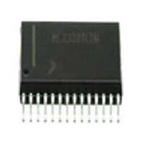
MC33742SDW Freescale, MC33742SDW Datasheet - Page 52

MC33742SDW
Manufacturer Part Number
MC33742SDW
Description
Manufacturer
Freescale
Datasheet
1.MC33742SDW.pdf
(70 pages)
Specifications of MC33742SDW
Data Rate
1000Kbps
Number Of Transceivers
1
Standard Supported
CAN 2.0
Operating Supply Voltage (max)
27V
Operating Supply Voltage (typ)
5/9/12/15/18/24V
Operating Supply Voltage (min)
4.5V
Package Type
SOIC W
Supply Current
45mA
Operating Temperature (max)
125C
Operating Temperature (min)
-40C
Operating Temperature Classification
Automotive
Mounting
Surface Mount
Pin Count
28
Lead Free Status / RoHS Status
Not Compliant
Available stocks
Company
Part Number
Manufacturer
Quantity
Price
Part Number:
MC33742SDW
Manufacturer:
MOTOROLA/摩托罗拉
Quantity:
20 000
Table 28. Wake-up Register Control Bits
Table 29. Wake-up Register Status Bits
TIMING REGISTER (TIM1 / 2)
• TIM1 — Controls the watchdog timing selection as well as either the watchdog window or the watchdog timeout option
• TIM2 — Selects an appropriate timing for sensing the wake-up circuitry or cyclically supplying devices by switching the HS on
Table 30. TIM1 Timing and CANL Failure Diagnostic Register
52
33742
FUNCTIONAL DEVICE OPERATION
LOGIC COMMANDS AND REGISTERS
x = Don’t care.
Notes
Notes
62.
63.
Tables 30
(
described in
or off. TIM2 is selected when bit D3 is 1
Cyclic sense timing characteristics are described in
Both subregisters also report the CANL and TXD diagnostics.
Figure 28
Reset Condition
LCTR3
Reset Value
(Write)
WUR status bits have two functions. After SBC wake-up, they indicate the wake-up source; for example, L2WU set at logic [1] if wake-
up source is L2 input. After SBC wake-up and once the WUR register has been read, status bits indicate the real-time state of the Lx
inputs (1 = Lx is above threshold, 0 = Lx input is below threshold). If after a wake-up from Lx input a watchdog timeout occurs before the
first reading of the WUR register, the LxWU bits are reset. This can occur only if the SBC was in Stop mode.
See
0
0
1
1
x
x
x
x
$101b
TIM1
L3WU
L2WU
L1WU
L0WU
Name
Table
and
(63)
through
Table
13, page 47, for definitions of reset conditions.
Figure 29
34
31.
LCTR2
contain the Timing Register information. The TIM register is composed of two sub registers:
0
1
0
1
x
x
x
x
, respectively). TIM1 is selected when bit D3 is 0
R/W
W
R
–
–
Logic
0 or 1
0 or 1
0 or 1
0 or 1
LCTR1
0
0
1
1
x
x
x
x
(Table
CANL2VDD
(62)
D3
0
–
–
32).
Figure
Table
If bit = 1, wake-up occurred from Sleep or Stop modes; if bit = 0, no wake-up has
occurred.
When device is in Normal or Standby mode, bit reports the State on Lx pin (LOW
or HIGH) (0 = Lx LOW, 1 = Lx HIGH)
LCTR0
0
1
0
1
x
x
x
x
30, page 54, describes HS operation when cyclic sense is selected
34, page 54.
POR, RESET
CANL2BAT
WDW
D2
0
L0 L1 : L1 L2 Config
High Level Sensitive
Both Level Sensitive
Low Level Sensitive
(Table
Inputs Disabled
–
30). Watchdog timing characteristics are
Description
Analog Integrated Circuit Device Data
POR, RESET
CANL2GND
WDT1
D1
0
Freescale Semiconductor
L2 L3 : L3 L4 Config
High Level Sensitive
Both Level Sensitive
Low Level Sensitive
Inputs Disabled
–
POR, RESET
WDT0
TXPD
D0
0


