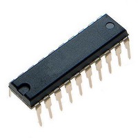
ETC5064N/C STMicroelectronics, ETC5064N/C Datasheet - Page 4

ETC5064N/C
Manufacturer Part Number
ETC5064N/C
Description
RF Wireless Misc Interfc CODEC Filter
Manufacturer
STMicroelectronics
Type
Telecom IC'sr
Datasheet
1.ETC5064DC013TR.pdf
(18 pages)
Specifications of ETC5064N/C
Operating Frequency
2.048 MHz
Operating Temperature Range
- 25 C to + 125 C
Package / Case
DIP-20
Mounting Style
Through Hole
Lead Free Status / RoHS Status
Lead free / RoHS Compliant
Available stocks
Company
Part Number
Manufacturer
Quantity
Price
Company:
Part Number:
ETC5064N/C
Manufacturer:
STM
Quantity:
861
Part Number:
ETC5064N/C
Manufacturer:
ST
Quantity:
20 000
ETC5064 - ETC5064-X - ETC5067 - ETC5067-X
4/18
FUNCTIONAL DESCRIPTION
POWER-UP
When power is first applied, power-on reset circuitry
initializes the device and places it into the power-
down mode. All non-essential circuits are deacti-
vated and the D
impedance states. To power-up the device, a logical
low level or clock must be applied to the
MCLK
be present. Thus 2 power-down control modes are
available. The first is to pull the MCLK
high; the alternative is to hold both FS
puts continuously low. The device will power-down
approximately 2 ms after the last FS
TRI-STATE PCM data output, D
high impedance state until the second FS
SYNCHRONOUS OPERATION
For synchronous operation, the same master clock
and bit clock should be used for both the transmit
and receive directions. In this mode, a clock must be
applied to MCLK
used as a power-down control. A low level on
MCLK
powers down the device. In either case, MCLKX will
be selected as the master clock for both the transmit
and receive circuits. A bit clock must also be applied
to BCLK
lect the proper internal divider for a master clock of
1.536 MHz, 1.544 MHz or 2.048 MHz. For 1.544
MHz operation, the device automatically compen-
sates for the 193 rd clock pulse each frame.
With a fixed level on the BCLK
will be selected as the bit clock for both the transmit
and receive directions. Table 1 indicates the fre-
quencies of operation which can be selected, de-
pending on the state of BCLK
chronous mode, the bit clock, BCLK
64 kHz to 2.048 MHz, but must be synchronous with
MCLK
Table 1: Selection of Master Clock Frequencies.
Clocked
0
1 (or open circuit)
BCLKR/CLKSEL
R
R
X
.
/PDN pin and FS
/PDN powers up the device and a high level
X
and the BCL
X
X
and VF
and the MCLK
R
1.536MHz or
ETC5067-X
/CLKSEL can be used to se-
2.048MHz
1.544MHz
2.048MHz
ETC5067
R
X
Frequency Selected
O outputs are put in high
and/or FS
R
Master Clock
R
/CLKSEL. In this syn-
/CKSEL pin, BCLK
X
, will remain in the
R
/PDN pin can be
X
R
, may be from
X
1.536MHz or
1.536MHz or
X
ETC5064-X
pulses must
1.544MHz
2.048MHz
1.544MHz
ETC5064
and FS
pulse. The
R
/PDN pin
X
pulse.
R
in-
X
Each FS
PCM data from the previous encode cycle is shift out
of the enabled D
BCLK
output is returned to a high impedance state. With an
FS
the negative edge of BCLK
FS
ASYNCHRONOUS OPERATION
For asynchronous operation, separate transmit and
receive clocks may be applied. MCLK
must be 2.048 MHz for the ETC5067 or 1.536 MHz,
1.544 MHz for the ETC5064, and need not be syn-
chronous. For best transmission performance, how-
ever, MCLK
which is easily achieved by applying only static logic
levels to the MCLK
connect MCLK
pin description). For 1.544 MHz operation, the de-
vice automatically compensates for the 193rd clock
pulse each frame. FS
and must be synchronous with MCLK
FS
chronous with BCLK
logic levels shown in Table 1 are not valid in asyn-
chronous mode. BCLK
from 64kHz to 2.048 MHz.
SHORT FRAME SYNC OPERATION
The device can utilize either a short frame sync
pulse or a long frame sync pulse. Upon power initiali-
zation, the device assumes a short frame mode. In
this mode, both frame sync pulses. FS
must be one bit clock period long, with timing rela-
tionships specified in figure 2. With FS
a falling edge of BCLK
BCLK
which will output the sign bit. The following seven ris-
ing edges clock out the remaining seven bits, and
the next falling edge disables the D
FS
synchronous mode), the next falling edge of BCLK
latches in the sign bit. The following seven falling
edges latch in the seven remaining bits. Both de-
vices may utilize the short frame sync pulse in syn-
chronous or asynchronous operating mode.
LONG FRAME SYNC OPERATION
To use the long frame mode, both the frame sync
pulses, FS
periods long, with timing relationships specified in
figure 3. Based on the transmit frame sync FS
device will sense whether short or long frame sync
R
X
R
R
and FS
pulse, PCM data is latched via the D
high during a falling edge of BCLK
starts each decoding cycle and must be syn-
X
X
. After 8 bit clock periods, the TRISTATE D
enables the D
X
X
pulse begins the encoding cycle and the
R
and FS
R
must be synchronous with MCLKX/
should be synchronous with MCLK
X
to all internal MCLK
X
R
R
/PDN pin. This will automatically
output on the positive edge of
, must be three or more bit clock
R
. BCLK
X
X
X
starts each encoding cycle
R
TRI-STATE output buffer,
and BCLK
, the next rising edge of
X
(or on BCKL
R
must be a clock, the
R
R
X
functions (see
X
X
may operate
X
output. With
and BCLK
R
and MCLK
R
X
high during
(BCLK
if running).
R
and FS
input on
X
, the
X
R
.
R
X
X
in
R
R
X
,
.
,


