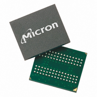
MT48LC4M32B2B5-7:G Micron Technology Inc, MT48LC4M32B2B5-7:G Datasheet - Page 57

MT48LC4M32B2B5-7:G
Manufacturer Part Number
MT48LC4M32B2B5-7:G
Description
DRAM Chip SDRAM 128M-Bit 4Mx32 3.3V 90-Pin VFBGA Tray
Manufacturer
Micron Technology Inc
Type
SDRAMr
Datasheet
1.MT48LC4M32B2P-7G_TR.pdf
(67 pages)
Specifications of MT48LC4M32B2B5-7:G
Density
128 Mb
Maximum Clock Rate
143 MHz
Package
90VFBGA
Address Bus Width
14 Bit
Operating Supply Voltage
3.3 V
Maximum Random Access Time
17|8|5.5 ns
Operating Temperature
0 to 70 °C
Format - Memory
RAM
Memory Type
SDRAM
Memory Size
128M (4Mx32)
Speed
143MHz
Interface
Parallel
Voltage - Supply
3 V ~ 3.6 V
Package / Case
90-VFBGA
Organization
4Mx32
Address Bus
14b
Access Time (max)
17/8/5.5ns
Operating Supply Voltage (typ)
3.3V
Package Type
VFBGA
Operating Temp Range
0C to 70C
Operating Supply Voltage (max)
3.6V
Operating Supply Voltage (min)
3V
Supply Current
175mA
Pin Count
90
Mounting
Surface Mount
Operating Temperature Classification
Commercial
Lead Free Status / RoHS Status
Lead free / RoHS Compliant
Lead Free Status / RoHS Status
Compliant, Lead free / RoHS Compliant
Available stocks
Company
Part Number
Manufacturer
Quantity
Price
Company:
Part Number:
MT48LC4M32B2B5-7:G
Manufacturer:
Micron Technology Inc
Quantity:
10 000
Company:
Part Number:
MT48LC4M32B2B5-7:G TR
Manufacturer:
Micron Technology Inc
Quantity:
10 000
Figure 40:
PDF: 09005aef80872800/Source: 09005aef80863355
128MbSDRAMx32_2.fm - Rev. L 1/09 EN
COMMAND
A0–A9, A11
DQM 0–3
BA0, BA1
CLK
CKE
A10
DQ
t CMS
t CKS
t AS
t AS
t AS
Alternating Bank Read Accesses
ACTIVE
BANK 0
T0
ROW
ROW
t CKH
t CMH
t AH
t AH
t AH
Notes:
t RCD - BANK 0
t RAS - BANK 0
t
t
RC - BANK 0
RRD
t CK
T1
NOP
1. For this example, BL = 4, and CL = 2.
2. A8, A9, and A11 = “Don’t Care.”
ENABLE AUTO PRECHARGE
t CMS
t CL
COLUMN m 2
BANK 0
T2
READ
t CMH
t CH
CAS Latency - BANK 0
T3
NOP
t LZ
t AC
57
BANK 4
ACTIVE
T4
ROW
ROW
D
OUT
t OH
t AC
m
t RCD - BANK 4
Micron Technology, Inc., reserves the right to change products or specifications without notice.
D
T5
OUT
NOP
m + 1
t OH
t AC
ENABLE AUTO PRECHARGE
COLUMN b 2
BANK 4
D
T6
READ
OUT
m + 2
t OH
t AC
CAS Latency - BANK 4
t RP - BANK 0
©2001 Micron Technology, Inc. All rights reserved.
D
128Mb: x32 SDRAM
T7
OUT
NOP
m + 3
t OH
Timing Diagrams
t AC
BANK 0
T8
ROW
ACTIVE
ROW
D
OUT
t RCD - BANK 0
t OH
DON’T CARE
UNDEFINED
t AC
b


