MT48LC16M16A2BG-75:D Micron Technology Inc, MT48LC16M16A2BG-75:D Datasheet - Page 6
MT48LC16M16A2BG-75:D
Manufacturer Part Number
MT48LC16M16A2BG-75:D
Description
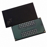
DRAM Chip SDRAM 256M-Bit 16Mx16 3.3V 54-Pin VFBGA Tray
Manufacturer
Micron Technology Inc
Type
SDRAMr
Specifications of MT48LC16M16A2BG-75:D
Density
256 Mb
Maximum Clock Rate
133 MHz
Package
54VFBGA
Address Bus Width
15 Bit
Operating Supply Voltage
3.3 V
Maximum Random Access Time
6|5.4 ns
Operating Temperature
0 to 70 °C
Format - Memory
RAM
Memory Type
SDRAM
Memory Size
256M (16Mx16)
Speed
133MHz
Interface
Parallel
Voltage - Supply
3 V ~ 3.6 V
Package / Case
54-VFBGA
Organization
16Mx16
Address Bus
15b
Access Time (max)
6/5.4ns
Operating Supply Voltage (typ)
3.3V
Package Type
VFBGA
Operating Temp Range
0C to 70C
Operating Supply Voltage (max)
3.6V
Operating Supply Voltage (min)
3V
Supply Current
135mA
Pin Count
54
Mounting
Surface Mount
Operating Temperature Classification
Commercial
Lead Free Status / RoHS Status
Lead free / RoHS Compliant
Lead Free Status / RoHS Status
Compliant, Lead free / RoHS Compliant
Available stocks
Company
Part Number
Manufacturer
Quantity
Price
Company:

Part Number:
MT48LC16M16A2BG-75:D
Manufacturer:
Micron Technology Inc
Quantity:
10 000
Company:
Part Number:
MT48LC16M16A2BG-75:D TR
Manufacturer:
Micron Technology Inc
Quantity:
10 000


256Mb: x4, x8, x16 SDRAM
List of Figures
Figure 1: 64 Meg x 4 Functional Block Diagram ................................................................................................ 9
Figure 2: 32 Meg x 8 Functional Block Diagram .............................................................................................. 10
Figure 3: 16 Meg x 16 Functional Block Diagram ............................................................................................. 11
Figure 4: 54-Pin TSOP (Top View) .................................................................................................................. 12
Figure 5: 60-Ball FBGA (Top View) ................................................................................................................. 13
Figure 6: 54-Ball VFBGA (Top View) ............................................................................................................... 14
Figure 7: 54-Pin Plastic TSOP (400 mil) ........................................................................................................... 16
Figure 8: 60-Ball FBGA "FB" (8mm x 16mm) (x4, x8) ....................................................................................... 17
Figure 9: 54-Ball VFBGA "FG" (8mm x 14mm) (x16) ........................................................................................ 18
Figure 10: Example: Temperature Test Point Location, 54-Pin TSOP (Top View) .............................................. 20
Figure 11: Example: Temperature Test Point Location, 54-Ball VFBGA (Top View) ........................................... 21
Figure 12: Example: Temperature Test Point Location, 60-Ball FBGA (Top View) ............................................. 21
Figure 13: ACTIVE Command ........................................................................................................................ 33
Figure 14: READ Command ........................................................................................................................... 34
Figure 15: WRITE Command ......................................................................................................................... 35
Figure 16: PRECHARGE Command ................................................................................................................ 36
Figure 17: Initialize and Load Mode Register .................................................................................................. 45
Figure 18: Mode Register Definition ............................................................................................................... 47
Figure 19: CAS Latency .................................................................................................................................. 50
t
t
t
Figure 20: Example: Meeting
RCD (MIN) When 2 <
RCD (MIN)/
CK < 3 ......................................................... 51
Figure 21: Consecutive READ Bursts .............................................................................................................. 53
Figure 22: Random READ Accesses ................................................................................................................ 54
Figure 23: READ-to-WRITE ............................................................................................................................ 55
Figure 24: READ-to-WRITE With Extra Clock Cycle ......................................................................................... 56
Figure 25: READ-to-PRECHARGE .................................................................................................................. 56
Figure 26: Terminating a READ Burst ............................................................................................................. 57
Figure 27: Alternating Bank Read Accesses ..................................................................................................... 58
Figure 28: READ Continuous Page Burst ........................................................................................................ 59
Figure 29: READ – DQM Operation ................................................................................................................ 60
Figure 30: WRITE Burst ................................................................................................................................. 61
Figure 31: WRITE-to-WRITE .......................................................................................................................... 62
Figure 32: Random WRITE Cycles .................................................................................................................. 63
Figure 33: WRITE-to-READ ............................................................................................................................ 63
Figure 34: WRITE-to-PRECHARGE ................................................................................................................. 64
Figure 35: Terminating a WRITE Burst ........................................................................................................... 65
Figure 36: Alternating Bank Write Accesses .................................................................................................... 66
Figure 37: WRITE – Continuous Page Burst .................................................................................................... 67
Figure 38: WRITE – DQM Operation ............................................................................................................... 68
Figure 39: READ With Auto Precharge Interrupted by a READ ......................................................................... 70
Figure 40: READ With Auto Precharge Interrupted by a WRITE ....................................................................... 71
Figure 41: READ With Auto Precharge ............................................................................................................ 72
Figure 42: READ Without Auto Precharge ....................................................................................................... 73
Figure 43: Single READ With Auto Precharge .................................................................................................. 74
Figure 44: Single READ Without Auto Precharge ............................................................................................. 75
Figure 45: WRITE With Auto Precharge Interrupted by a READ ....................................................................... 76
Figure 46: WRITE With Auto Precharge Interrupted by a WRITE ...................................................................... 76
Figure 47: WRITE With Auto Precharge .......................................................................................................... 77
Figure 48: WRITE Without Auto Precharge ..................................................................................................... 78
Figure 49: Single WRITE With Auto Precharge ................................................................................................ 79
Figure 50: Single WRITE Without Auto Precharge ........................................................................................... 80
6
PDF: 09005aef8091e6d1
Micron Technology, Inc. reserves the right to change products or specifications without notice.
256Mb_sdr.pdf - Rev. N 1/10 EN
© 1999 Micron Technology, Inc. All rights reserved.
Related parts for MT48LC16M16A2BG-75:D
Image
Part Number
Description
Manufacturer
Datasheet
Request
R

Part Number:
Description:
IC SDRAM 64MBIT 133MHZ 54TSOP
Manufacturer:
Micron Technology Inc
Datasheet:

Part Number:
Description:
IC SDRAM 64MBIT 5.5NS 86TSOP
Manufacturer:
Micron Technology Inc
Datasheet:
Part Number:
Description:
IC SDRAM 64MBIT 200MHZ 86TSOP
Manufacturer:
Micron Technology Inc
Datasheet:
Part Number:
Description:
IC SDRAM 64MBIT 133MHZ 54TSOP
Manufacturer:
Micron Technology Inc
Datasheet:
Part Number:
Description:
IC SDRAM 128MBIT 133MHZ 54TSOP
Manufacturer:
Micron Technology Inc
Datasheet:

Part Number:
Description:
IC SDRAM 256MBIT 133MHZ 90VFBGA
Manufacturer:
Micron Technology Inc
Datasheet:
Part Number:
Description:
IC SDRAM 128MBIT 133MHZ 54TSOP
Manufacturer:
Micron Technology Inc
Datasheet:
Part Number:
Description:
IC SDRAM 256MBIT 133MHZ 54TSOP
Manufacturer:
Micron Technology Inc
Datasheet:

Part Number:
Description:
IC DDR SDRAM 512MBIT 6NS 66TSOP
Manufacturer:
Micron Technology Inc
Datasheet:
Part Number:
Description:
IC SDRAM 128MBIT 167MHZ 86TSOP
Manufacturer:
Micron Technology Inc
Datasheet:
Part Number:
Description:
IC SDRAM 128MBIT 143MHZ 86TSOP
Manufacturer:
Micron Technology Inc
Datasheet:

Part Number:
Description:
SDRAM 256M-BIT 1.8V 54-PIN VFBGA
Manufacturer:
Micron Technology Inc
Datasheet:
Part Number:
Description:
IC SDRAM 128MBIT 143MHZ 86TSOP
Manufacturer:
Micron Technology Inc
Datasheet:

Part Number:
Description:
IC SDRAM 128MBIT 125MHZ 54VFBGA
Manufacturer:
Micron Technology Inc
Datasheet:
Part Number:
Description:
IC SDRAM 128MBIT 125MHZ 54VFBGA
Manufacturer:
Micron Technology Inc
Datasheet: