BLF6G38-50,112 NXP Semiconductors, BLF6G38-50,112 Datasheet - Page 6
BLF6G38-50,112
Manufacturer Part Number
BLF6G38-50,112
Description
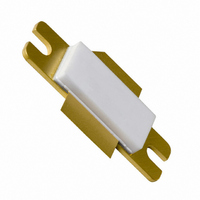
IC WIMAX 3.8GHZ SOT502A
Manufacturer
NXP Semiconductors
Datasheet
1.BLF6G38-50135.pdf
(13 pages)
Specifications of BLF6G38-50,112
Package / Case
SOT502A
Transistor Type
LDMOS
Frequency
3.4GHz ~ 3.6GHz
Gain
14dB
Voltage - Rated
65V
Current Rating
16.5A
Current - Test
450mA
Voltage - Test
28V
Power - Output
9W
Configuration
Single
Transistor Polarity
N-Channel
Resistance Drain-source Rds (on)
0.29 Ohms
Drain-source Breakdown Voltage
65 V
Gate-source Breakdown Voltage
13 V
Continuous Drain Current
16.5 A
Maximum Operating Temperature
+ 225 C
Mounting Style
SMD/SMT
Minimum Operating Temperature
- 65 C
Channel Type
N
Channel Mode
Enhancement
Drain Source Voltage (max)
65V
Output Power (max)
70W(Typ)
Power Gain (typ)@vds
14@28VdB
Frequency (min)
3.4GHz
Frequency (max)
3.6GHz
Package Type
LDMOST
Pin Count
3
Forward Transconductance (typ)
5.6S
Drain Source Resistance (max)
290@6.15Vmohm
Reverse Capacitance (typ)
1.17@28VpF
Operating Temp Range
-65C to 200C
Drain Efficiency (typ)
23%
Mounting
Screw
Mode Of Operation
1-Carrier N-CDMA
Number Of Elements
1
Vswr (max)
10
Screening Level
Military
Lead Free Status / RoHS Status
Lead free / RoHS Compliant
Noise Figure
-
Lead Free Status / Rohs Status
Compliant
Other names
934061173112
BLF6G38-50
BLF6G38-50
BLF6G38-50
BLF6G38-50


NXP Semiconductors
BLF6G38-50_BLF6G38LS-50
Product data sheet
Fig 6.
Fig 8.
(dB)
(dB)
G
G
(1) f = 3400 MHz
(2) f = 3500 MHz
(3) f = 3600 MHz
p
p
18
16
14
12
10
16
15
14
13
12
10
10
V
N-CDMA; PAR = 9.7 dB at 0.01 % probability; Channel
Bandwidth = 1.23 MHz; IBW = 30 kHz.
Power gain and drain efficiency as functions
of load power; typical values
V
PAR = 9.7 dB at 0.01 % probability; Channel Bandwidth
= 1.23 MHz; IBW = 30 kHz.
Power gain as a function of load power; typical
values
−1
−1
DS
DS
= 28 V; I
= 28 V; I
Dq
Dq
1
1
= 450 mA; f = 3500 MHz; Single Carrier
= 450 mA; Single Carrier N-CDMA;
G
η
(2)
(1)
(3)
D
p
10
10
P
P
All information provided in this document is subject to legal disclaimers.
L
L
001aah400
001aah402
(W)
(W)
10
10
Rev. 02 — 1 June 2010
2
2
40
30
20
10
0
(%)
η
D
BLF6G38-50; BLF6G38LS-50
Fig 7.
Fig 9.
ACPR
(dBc)
(W)
P
(1) Low frequency component
(2) High frequency component
(1) f = 3400 MHz
(2) f = 3500 MHz
(3) f = 3600 MHz
−30
−40
−50
−60
−70
−80
i
1.5
1.0
0.5
0
10
10
V
N-CDMA; PAR = 9.7 dB at 0.01 % probability; Channel
Bandwidth = 1.23 MHz; IBW = 30 kHz.
Adjacent channel power ratio as a function of
load power; typical values
V
PAR = 9.7 dB at 0.01 % probability; Channel Bandwidth
= 1.23 MHz; IBW = 30 kHz.
Input power as a function of load power;
typical values
−1
−1
DS
DS
ACPR
ACPR
ACPR
= 28 V; I
= 28 V; I
885k
1500k
1980k
Dq
Dq
WiMAX power LDMOS transistor
1
1
= 450 mA; f = 3500 MHz; Single Carrier
= 450 mA; Single Carrier N-CDMA;
(1)
(2)
(1)
(2)
(3)
(2)
(1)
(1)
(2)
10
10
© NXP B.V. 2010. All rights reserved.
P
P
L
L
001aah401
001aah403
(W)
(W)
10
10
2
2
6 of 13
Related parts for BLF6G38-50,112
Image
Part Number
Description
Manufacturer
Datasheet
Request
R

Part Number:
Description:
100 W LDMOS power transistor for base station applications at frequencies from 3400 MHz to 3600 MHz
Manufacturer:
NXP Semiconductors
Datasheet:

Part Number:
Description:
RF MOSFET Small Signal LDMOS TNS
Manufacturer:
NXP Semiconductors
Datasheet:

Part Number:
Description:
RF MOSFET Small Signal LDMOS TNS
Manufacturer:
NXP Semiconductors
Datasheet:

Part Number:
Description:
RF MOSFET Small Signal LDMOS TNS
Manufacturer:
NXP Semiconductors
Datasheet:

Part Number:
Description:
IC WIMAX 3.8GHZ 2-LDMOST
Manufacturer:
NXP Semiconductors
Datasheet:

Part Number:
Description:
IC WIMAX 3.8GHZ SOT608A
Manufacturer:
NXP Semiconductors
Datasheet:

Part Number:
Description:
RF MOSFET Small Signal LDMOS TNS
Manufacturer:
NXP Semiconductors
Datasheet:
Part Number:
Description:
RF MOSFET Small Signal LDMOS TNS
Manufacturer:
NXP Semiconductors
Datasheet:
Part Number:
Description:
RF MOSFET Small Signal LDMOS TNS
Manufacturer:
NXP Semiconductors
Part Number:
Description:
IC WIMAX 3.8GHZ 2-LDMOST
Manufacturer:
NXP Semiconductors
Datasheet:
Part Number:
Description:
IC WIMAX 3.8GHZ 2-LDMOST
Manufacturer:
NXP Semiconductors
Datasheet:
Part Number:
Description:
IC WIMAX 3.8GHZ 2-LDMOST
Manufacturer:
NXP Semiconductors
Datasheet:
Part Number:
Description:
TRANS WIMAX PWR LDMOS SOT502A
Manufacturer:
NXP Semiconductors
Datasheet:

Part Number:
Description:
TRANS WIMAX PWR LDMOS SOT502A
Manufacturer:
NXP Semiconductors
Datasheet:
Part Number:
Description:
NXP Semiconductors designed the LPC2420/2460 microcontroller around a 16-bit/32-bitARM7TDMI-S CPU core with real-time debug interfaces that include both JTAG andembedded trace
Manufacturer:
NXP Semiconductors
Datasheet: