BLF6G38-50,112 NXP Semiconductors, BLF6G38-50,112 Datasheet - Page 3
BLF6G38-50,112
Manufacturer Part Number
BLF6G38-50,112
Description
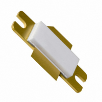
IC WIMAX 3.8GHZ SOT502A
Manufacturer
NXP Semiconductors
Datasheet
1.BLF6G38-50135.pdf
(13 pages)
Specifications of BLF6G38-50,112
Package / Case
SOT502A
Transistor Type
LDMOS
Frequency
3.4GHz ~ 3.6GHz
Gain
14dB
Voltage - Rated
65V
Current Rating
16.5A
Current - Test
450mA
Voltage - Test
28V
Power - Output
9W
Configuration
Single
Transistor Polarity
N-Channel
Resistance Drain-source Rds (on)
0.29 Ohms
Drain-source Breakdown Voltage
65 V
Gate-source Breakdown Voltage
13 V
Continuous Drain Current
16.5 A
Maximum Operating Temperature
+ 225 C
Mounting Style
SMD/SMT
Minimum Operating Temperature
- 65 C
Channel Type
N
Channel Mode
Enhancement
Drain Source Voltage (max)
65V
Output Power (max)
70W(Typ)
Power Gain (typ)@vds
14@28VdB
Frequency (min)
3.4GHz
Frequency (max)
3.6GHz
Package Type
LDMOST
Pin Count
3
Forward Transconductance (typ)
5.6S
Drain Source Resistance (max)
290@6.15Vmohm
Reverse Capacitance (typ)
1.17@28VpF
Operating Temp Range
-65C to 200C
Drain Efficiency (typ)
23%
Mounting
Screw
Mode Of Operation
1-Carrier N-CDMA
Number Of Elements
1
Vswr (max)
10
Screening Level
Military
Lead Free Status / RoHS Status
Lead free / RoHS Compliant
Noise Figure
-
Lead Free Status / Rohs Status
Compliant
Other names
934061173112
BLF6G38-50
BLF6G38-50
BLF6G38-50
BLF6G38-50


NXP Semiconductors
5. Thermal characteristics
6. Characteristics
7. Application information
BLF6G38-50_BLF6G38LS-50
Product data sheet
7.1 Ruggedness in class-AB operation
Table 5.
Table 6.
T
Table 7.
Mode of operation: 1-carrier N-CDMA; Single carrier N-CDMA with pilot, paging, sync and 6 traffic
channels (Walsh codes 8 - 13). PAR = 9.7 dB at 0.01 % probability on the CCDF; Channel
bandwidth is 1.23 MHz; f
V
circuit.
[1]
The BLF6G38-50 and BLF6G38LS-50 are capable of withstanding a load mismatch
corresponding to VSWR = 10 : 1 through all phases under the following conditions:
V
Symbol
R
Symbol Parameter
V
V
I
I
I
g
R
C
Symbol
P
G
RL
η
ACPR
ACPR
DSS
DSX
GSS
j
DS
DS
fs
D
(BR)DSS
GS(th)
L(M)
th(j-case)
DS(on)
rs
p
= 25
in
= 28 V; I
Measured within 30 kHz bandwidth.
= 28 V; I
885k
1980k
°
C per section; unless otherwise specified.
drain-source breakdown voltage V
gate-source threshold voltage
drain leakage current
drain cut-off current
gate leakage current
forward transconductance
drain-source on-state resistance V
feedback capacitance
Thermal characteristics
Characteristics
Application information
Dq
Parameter
peak output power
power gain
input return loss
drain efficiency
adjacent channel power ratio (885 kHz)
adjacent channel power ratio (1980 kHz) P
Parameter
thermal resistance from
junction to case
Dq
= 450 mA; T
= 450 mA; P
All information provided in this document is subject to legal disclaimers.
1
= 3400 MHz; f
Rev. 02 — 1 June 2010
case
BLF6G38-50; BLF6G38LS-50
L
= 25
= P
L(1dB)
°
C; unless otherwise specified, in a class-AB production
Conditions
T
P
2
case
L
= 3500 MHz; f
; f = 3600 MHz.
= 50 W
Conditions
V
V
V
V
V
V
I
V
f = 1 MHz
= 80 °C;
D
GS
DS
GS
GS
DS
GS
DS
GS
GS
= 2.8 A
= 0 V; I
= 10 V; I
= 0 V; V
= V
= 10 V
= +11 V; V
= 10 V; I
= V
= 0 V; V
GS(th)
GS(th)
Conditions
P
P
P
P
P
3
D
L(AV)
L(AV)
L(AV)
L(AV)
L(AV)
L(AV)
= 3600 MHz; RF performance at
DS
DS
D
D
Type
BLF6G38-50
BLF6G38LS-50
= 0.4 mA
+ 3.75 V;
+ 3.75 V;
= 80 mA
= 2.8 A
DS
WiMAX power LDMOS transistor
= 28 V
= 28 V;
= 9 W
= 9 W
= 9 W
= 9 W
= 9 W
= 9 W
= 0 V
[1]
[1]
Min
65
1.4
-
11.8
-
-
-
-
Min
65
12.5 14
-
20
−46
−62
© NXP B.V. 2010. All rights reserved.
Typ
-
2
-
16.4
-
5.6
0.18
1.17
Typ
0.9
0.7
Typ
70
−10
23
−49
−64
Max
-
2.4
2.8
-
280
-
0.29
-
Max
-
-
-
-
-
-
Unit
-
-
3 of 13
Unit
W
dB
dB
%
dBc
dBc
Unit
V
V
μA
nA
S
Ω
pF
A
Related parts for BLF6G38-50,112
Image
Part Number
Description
Manufacturer
Datasheet
Request
R

Part Number:
Description:
100 W LDMOS power transistor for base station applications at frequencies from 3400 MHz to 3600 MHz
Manufacturer:
NXP Semiconductors
Datasheet:

Part Number:
Description:
RF MOSFET Small Signal LDMOS TNS
Manufacturer:
NXP Semiconductors
Datasheet:

Part Number:
Description:
RF MOSFET Small Signal LDMOS TNS
Manufacturer:
NXP Semiconductors
Datasheet:

Part Number:
Description:
RF MOSFET Small Signal LDMOS TNS
Manufacturer:
NXP Semiconductors
Datasheet:

Part Number:
Description:
IC WIMAX 3.8GHZ 2-LDMOST
Manufacturer:
NXP Semiconductors
Datasheet:

Part Number:
Description:
IC WIMAX 3.8GHZ SOT608A
Manufacturer:
NXP Semiconductors
Datasheet:

Part Number:
Description:
RF MOSFET Small Signal LDMOS TNS
Manufacturer:
NXP Semiconductors
Datasheet:
Part Number:
Description:
RF MOSFET Small Signal LDMOS TNS
Manufacturer:
NXP Semiconductors
Datasheet:
Part Number:
Description:
RF MOSFET Small Signal LDMOS TNS
Manufacturer:
NXP Semiconductors
Part Number:
Description:
IC WIMAX 3.8GHZ 2-LDMOST
Manufacturer:
NXP Semiconductors
Datasheet:
Part Number:
Description:
IC WIMAX 3.8GHZ 2-LDMOST
Manufacturer:
NXP Semiconductors
Datasheet:
Part Number:
Description:
IC WIMAX 3.8GHZ 2-LDMOST
Manufacturer:
NXP Semiconductors
Datasheet:
Part Number:
Description:
TRANS WIMAX PWR LDMOS SOT502A
Manufacturer:
NXP Semiconductors
Datasheet:

Part Number:
Description:
TRANS WIMAX PWR LDMOS SOT502A
Manufacturer:
NXP Semiconductors
Datasheet:
Part Number:
Description:
NXP Semiconductors designed the LPC2420/2460 microcontroller around a 16-bit/32-bitARM7TDMI-S CPU core with real-time debug interfaces that include both JTAG andembedded trace
Manufacturer:
NXP Semiconductors
Datasheet: