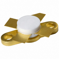
BLF245,112 NXP Semiconductors, BLF245,112 Datasheet - Page 4

BLF245,112
Manufacturer Part Number
BLF245,112
Description
TRANSISTOR RF DMOS SOT123A
Manufacturer
NXP Semiconductors
Datasheet
1.BLF245112.pdf
(16 pages)
Specifications of BLF245,112
Package / Case
SOT-123A
Transistor Type
N-Channel
Frequency
175MHz
Gain
15.5dB
Voltage - Rated
65V
Current Rating
6A
Noise Figure
2dB
Current - Test
50mA
Voltage - Test
28V
Power - Output
30W
Minimum Operating Temperature
- 65 C
Mounting Style
SMD/SMT
Resistance Drain-source Rds (on)
0.75 Ohm @ 10 V
Transistor Polarity
N-Channel
Configuration
Single Dual Source
Drain-source Breakdown Voltage
65 V
Gate-source Breakdown Voltage
+/- 20 V
Continuous Drain Current
6 A
Power Dissipation
68000 mW
Maximum Operating Temperature
+ 200 C
Application
VHF
Channel Type
N
Channel Mode
Enhancement
Drain Source Voltage (max)
65V
Output Power (max)
30W
Power Gain (typ)@vds
15.5@28V/12@12.5VdB
Noise Figure (max)
2(Typ)dB
Frequency (max)
175MHz
Package Type
SOT-123A
Pin Count
4
Forward Transconductance (typ)
1.9S
Drain Source Resistance (max)
750@10Vmohm
Input Capacitance (typ)@vds
125@28VpF
Output Capacitance (typ)@vds
75@28VpF
Reverse Capacitance (typ)
7@28VpF
Operating Temp Range
-65C to 200C
Drain Efficiency (typ)
67%
Mounting
Screw
Mode Of Operation
CW Class-B
Number Of Elements
1
Power Dissipation (max)
68000mW
Vswr (max)
50
Screening Level
Military
Lead Free Status / RoHS Status
Lead free / RoHS Compliant
Lead Free Status / RoHS Status
Lead free / RoHS Compliant, Lead free / RoHS Compliant
Other names
568-2402
933817060112
BLF245
BLF245
933817060112
BLF245
BLF245
Philips Semiconductors
CHARACTERISTICS
T
V
2003 Sep 02
V
I
I
V
g
R
I
C
C
C
F
j
DSS
GSS
DSX
GS
SYMBOL
fs
V
(BR)DSS
GSth
= 25 C unless otherwise specified.
DSon
is
os
rs
VHF power MOS transistor
GS
group indicator
GROUP
M
C
D
G
H
N
A
B
E
F
K
J
L
drain-source breakdown voltage
drain-source leakage current
gate-source leakage current
gate-source threshold voltage
gate-source voltage difference of
matched devices
forward transconductance
drain-source on-state resistance
on-state drain current
input capacitance
output capacitance
feedback capacitance
noise figure
PARAMETER
MIN.
2.0
2.1
2.2
2.3
2.4
2.5
2.6
2.7
2.8
2.9
3.0
3.1
3.2
LIMITS
(V)
MAX.
2.1
2.2
2.3
2.4
2.5
2.6
2.7
2.8
2.9
3.0
3.1
3.2
3.3
V
V
V
I
I
I
I
V
V
V
V
input and output power matched for:
I
R1 = 1 k ; T
see Fig.14
D
D
D
D
D
GS
GS
GS
GS
GS
GS
GS
= 10 mA; V
= 0 mA; V
= 1.5 A; V
= 1.5 A; V
= 1 A; V
= 0; I
= 0; V
= 20 V; V
= 10 V; V
= 0; V
= 0; V
= 0; V
4
D
DS
DS
DS
DS
DS
= 10 mA
CONDITIONS
DS
DS
GS
h
= 28 V
= 28 V; f = 1 MHz
= 28 V; f = 1 MHz
= 28 V; f = 1 MHz
= 28 V; P
DS
DS
= 25 C; f = 175 MHz;
GROUP
DS
= 10 V
= 10 V
= 10 V
= 10 V
= 10 V
W
= 0
O
Q
R
U
P
S
T
V
X
Y
Z
L
= 30 W;
MIN.
3.3
3.4
3.5
3.6
3.7
3.8
3.9
4.0
4.1
4.2
4.3
4.4
65
2
1.2
MIN. TYP. MAX. UNIT
LIMITS
(V)
1.9
0.4
10
125
75
7
2
Product specification
BLF245
2
1
4.5
100
0.75
MAX.
3.4
3.5
3.6
3.7
3.8
3.9
4.0
4.1
4.2
4.3
4.4
4.5
V
mA
V
mV
S
A
pF
pF
pF
dB
A


