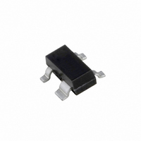
BF1211,215 NXP Semiconductors, BF1211,215 Datasheet - Page 7

BF1211,215
Manufacturer Part Number
BF1211,215
Description
MOSFET N-CH DUAL GATE 6V SOT143B
Manufacturer
NXP Semiconductors
Datasheet
1.BF1211215.pdf
(16 pages)
Specifications of BF1211,215
Package / Case
SOT-143, SOT-143B, TO-253AA
Transistor Type
N-Channel Dual Gate
Frequency
400MHz
Gain
29dB
Voltage - Rated
6V
Current Rating
30mA
Noise Figure
0.9dB
Current - Test
15mA
Voltage - Test
5V
Configuration
Single Dual Gate
Continuous Drain Current
0.03 A
Drain-source Breakdown Voltage
6 V
Gate-source Breakdown Voltage
6 V
Maximum Operating Temperature
+ 150 C
Minimum Operating Temperature
- 65 C
Mounting Style
SMD/SMT
Power Dissipation
180 mW
Transistor Polarity
N-Channel
Application
VHF/UHF
Channel Type
N
Channel Mode
Enhancement
Drain Source Voltage (max)
6V
Power Gain (typ)@vds
34@5VdB
Noise Figure (max)
2dB
Package Type
SOT
Pin Count
3 +Tab
Input Capacitance (typ)@vds
2.1@5V@Gate 1/1.1@5V@Gate 2pF
Output Capacitance (typ)@vds
0.9@5VpF
Reverse Capacitance (typ)
0.015@5VpF
Operating Temp Range
-65C to 150C
Mounting
Surface Mount
Number Of Elements
2
Power Dissipation (max)
180mW
Screening Level
Military
Lead Free Status / RoHS Status
Lead free / RoHS Compliant
Power - Output
-
Lead Free Status / Rohs Status
Lead free / RoHS Compliant
Other names
568-1959-2
934057516215
BF1211
934057516215
BF1211
NXP Semiconductors
2003 Dec 16
handbook, halfpage
handbook, halfpage
N-channel dual-gate MOS-FETs
Fig.9
Fig.11 Drain current as a function of gate 1 (V
V
T
V
(1) R
(2) R
(3) R
(mA)
(mA)
j
DS
G2-S
I D
I D
= 25 C.
= 5 V; V
20
16
12
20
16
12
8
4
0
= 4 V; T
8
4
0
G1
G1
G1
0
0
= 47 k.
= 56 k.
= 68 k.
Drain current as a function of gate 1 current;
typical values.
and drain supply voltage; typical values.
G2-S
j
= 25 C; R
= 4 V.
10
(4) R
(5) R
(6) R
2
G1
20
connected to V
G1
G1
G1
= 75 k.
= 82 k.
= 100 k.
30
4
(1)
GG
V GG = V DS (V)
; see Fig.21.
(7) R
40
I G1 (μA)
(2)
(3)
(4)
(5)
(6)
(7)
MDB835
MDB833
G1
= 120 k.
50
6
GG
)
7
handbook, halfpage
handbook, halfpage
V
R
Fig.10 Drain current as a function of gate 1 supply
Fig.12 Drain current as a function of gate 2
V
(1) V
(2) V
(3) V
(mA)
(mA)
DS
G1
DS
I D
I D
= 5 V; V
= 75 k (connected to V
= 5 V; T
16
12
20
16
12
8
4
0
8
4
0
GG
GG
GG
BF1211; BF1211R; BF1211WR
0
0
= 5 V.
= 4.5 V.
= 4 V.
voltage (V
voltage; typical values.
G2-S
j
= 25 C; R
= 4 V; T
1
GG
G1
j
2
= 25 C.
= 75 k (connected to V
); typical values.
2
GG
); see Fig.21.
(4) V
(5) V
3
4
GG
GG
Product specification
= 3.5 V.
= 3 V.
V G2-S (V)
(1)
(2)
(3)
(4)
(5)
4
V GG (V)
GG
MDB834
MDB836
); see Fig.21.
5
6


