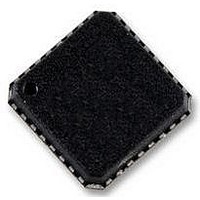
AD5748ACPZ Analog Devices Inc, AD5748ACPZ Datasheet - Page 4

AD5748ACPZ
Manufacturer Part Number
AD5748ACPZ
Description
ZDPLC +/-24V DRIVER
Manufacturer
Analog Devices Inc
Datasheet
1.AD5748ACPZ-RL7.pdf
(32 pages)
Specifications of AD5748ACPZ
Amplifier Type
Instrumentation
Number Of Circuits
1
Slew Rate
2 V/µs
Current - Output / Channel
15mA
Voltage - Supply, Single/dual (±)
±12 V ~ 24 V
Operating Temperature
-40°C ~ 105°C
Mounting Type
Surface Mount
Package / Case
*
No. Of Amplifiers
3
Supply Voltage Range
± 12V To ± 24V
Supply Current
5.2mA
Amplifier Case Style
LFCSP
No. Of Pins
32
Operating Temperature Range
-40°C To +105°C
Svhc
No
Rohs Compliant
Yes
Bandwidth
100kHz
Amplifier Output
Differential
Lead Free Status / RoHS Status
Lead free / RoHS Compliant
Output Type
-
Gain Bandwidth Product
-
-3db Bandwidth
-
Current - Input Bias
-
Voltage - Input Offset
-
Current - Supply
-
Lead Free Status / RoHS Status
Lead free / RoHS Compliant
AD5748
SPECIFICATIONS
AV
unless otherwise noted.
Table 2.
Parameter
INPUT VOLTAGE RANGE
REFERENCE INPUT
VOLTAGE OUTPUT, V
VOLTAGE OUTPUT CHARACTERISTICS
V
Input Leakage Current
Reference Input Voltage
Input Leakage Current
Output Voltage Ranges
Accuracy
Headroom
Short-Circuit Current
Load
Capacitive Load Stability
DC Output Impedance
0 V to 5 V range, ¼ to ¾ Step
0 V to 5 V range, 40 mV Input Step
Slew Rate
Output Noise
DD
IN
Total Unadjusted Error (TUE)
Relative Accuracy (INL)
Bipolar Zero Error (Offset at
Bipolar Zero Error TC
Zero-Scale Error
Zero-Scale Error TC
Zero-Scale/Offset Error
Offset Error TC
Gain Error
Gain Error TC
Full-Scale Error
Full-Scale Error TC
R
R
R
/AV
LOAD
LOAD
LOAD
Midscale)
SS
= ∞
= 2 kΩ
= ∞
1
= ±12 V (± 10%) to ±24 V (± 10%), DVCC = 2.7 V to 5.5 V, GND = 0 V. IOUT: R
3
3
OUT
3
3
3
2
3
Min
−1
−1
0
0
−10.5
−0.3
−0.1
−0.02
−10
−8
−10
−8
−5
−4
−3
−2.2
−0.05
−0.04
−0.05
−0.04
1
Typ
0 to 4.096
4.096
±0.05
±0.005
±0.5
±1.5
±0.5
±1
±0.5
±0.3
±2
±0.015
±0.5
±0.015
±1.5
15
0.12
2
45.5
7
4.5
2.5
Rev. A | Page 4 of 32
Max
+1
+1
5
10.5
+10.5
+0.3
+0.1
+0.02
+10
+8
+10
+8
+5
+4
+3
+2.2
+0.05
+0.04
+0.05
+0.04
1.3
1
1
2
Unit
V
μA
V
μA
V
V
V
% FSR
% FSR
% FSR
mV
mV
ppm FSR/°C
mV
mV
ppm FSR/°C
mV
mV
mV
mV
ppm FSR/°C
% FSR
% FSR
ppm FSR/°C
% FSR
% FSR
ppm FSR/°C
V
mA
kΩ
nF
nF
μF
Ω
μs
μs
V/μs
μV rms
μV rms
LOAD
= 300 Ω. All specifications T
Test Conditions/Comments
Output unloaded
External reference needs to be exactly as
stated; otherwise, accuracy errors show
up as error in output
AVDD must have minimum 1.3 V
headroom
AVDD/AVSS must have minimum 1.3 V
headroom
T
±10.5 V range
T
±10.5 V range
±10.5 V range
T
±10.5 V range
0 V to 10.5 V range
T
0 V to 5 V range
T
All ranges
T
All ranges
T
Output unloaded
T
External compensation capacitor required;
see the
Specified with 2 kΩ || 220 pF, ±0.05%
Specified with 2 kΩ || 220 pF, ±0.05%
Specified with 2 kΩ || 220 pF
0.1 Hz to 10 Hz bandwidth
100 kHz bandwidth
A
A
A
A
A
A
A
A
= 25°C
= 25°C, ±10.5 V range
= 25°C, ±10.5 V range
= 25°C, 0 V to 10.5 V range
= 25°C, 0 V to 5 V range
= 25°C
= 25°C
= 25°C
Driving Inductive Loads
MIN
to T
section
MAX
,


