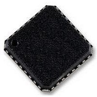
AD5748ACPZ Analog Devices Inc, AD5748ACPZ Datasheet - Page 30

AD5748ACPZ
Manufacturer Part Number
AD5748ACPZ
Description
ZDPLC +/-24V DRIVER
Manufacturer
Analog Devices Inc
Datasheet
1.AD5748ACPZ-RL7.pdf
(32 pages)
Specifications of AD5748ACPZ
Amplifier Type
Instrumentation
Number Of Circuits
1
Slew Rate
2 V/µs
Current - Output / Channel
15mA
Voltage - Supply, Single/dual (±)
±12 V ~ 24 V
Operating Temperature
-40°C ~ 105°C
Mounting Type
Surface Mount
Package / Case
*
No. Of Amplifiers
3
Supply Voltage Range
± 12V To ± 24V
Supply Current
5.2mA
Amplifier Case Style
LFCSP
No. Of Pins
32
Operating Temperature Range
-40°C To +105°C
Svhc
No
Rohs Compliant
Yes
Bandwidth
100kHz
Amplifier Output
Differential
Lead Free Status / RoHS Status
Lead free / RoHS Compliant
Output Type
-
Gain Bandwidth Product
-
-3db Bandwidth
-
Current - Input Bias
-
Voltage - Input Offset
-
Current - Supply
-
Lead Free Status / RoHS Status
Lead free / RoHS Compliant
AD5748
APPLICATIONS INFORMATION
TRANSIENT VOLTAGE PROTECTION
The AD5748 contains ESD protection diodes that prevent damage
from normal handling. The industrial control environment can,
however, subject I/O circuits to much higher transients. To protect
the AD5748 from excessively high voltage transients, external
power diodes and a surge current limiting resistor may be
required, as shown in Figure 54. The constraint on the resistor
value is that, during normal operation, the output level at IOUT
must remain within its voltage compliance limit of AV
and the two protection diodes and resistor must have appropri-
ate power ratings. Further protection can be added with transient
voltage suppressors if needed.
THERMAL CONSIDERATIONS
It is important to understand the effects of power dissipation
on the package and on junction temperature. The internal junction
temperature should not exceed 125°C. The AD5748 is packaged
in a 32-lead LFCSP 5, 5 mm × 5 mm package. The thermal
impedance, θ
not operated under conditions that cause the junction tempera-
ture to exceed its junction temperature.
Worst-case conditions occur when the AD5748 is operated from
the maximum AV
current (24 mA) directly to ground. The quiescent current of the
AD5748 should also be taken into account, nominally ~4 mA.
The following calculations estimate maximum power dissipation
under these worst-case conditions, and determine maximum
ambient temperature based on the power dissipation:
These figures assume that proper layout and grounding
techniques are followed to minimize power dissipation,
as outlined in the Layout Guidelines section.
Power Dissipation = 26.4 V × 28 mA = 0.7392 W
Temp Increase = 28°C × 0.7392 W = 20.7°C
Maximum Ambient Temp = 125°C − 20.7°C = 104.3°C
Figure 54. Output Transient Voltage Protection
JA
, is 28°C/W. It is important that the devices are
DD
AD5748
(26.4 V) while driving the maximum
AVDD
AVDD
AVSS
IOUT
R
P
R
LOAD
DD
− 2.75 V,
Rev. A | Page 30 of 32
LAYOUT GUIDELINES
In any circuit where accuracy is important, careful consideration
of the power supply and ground return layout helps to ensure
the rated performance. The PCB on which the AD5748 is
mounted should be designed so that the AD5748 lies on the
analog plane.
The AD5748 should have ample supply bypassing of 10 μF
in parallel with 0.1 μF on each supply located as close to the
package as possible, ideally right up against the device. The
10 μF capacitors are the tantalum bead type. The 0.1 μF capaci-
tor should have low effective series resistance (ESR) and low
effective series inductance (ESI) such as the common ceramic
types, which provide a low impedance path to ground at high
frequencies to handle transient currents due to internal logic
switching.
In systems where there are many devices on one board, it is often
useful to provide some heat sinking capability to allow the power
to dissipate easily.
The AD5748 has an exposed paddle beneath the device. This
paddle is connected to the AVSS supply for the part. For opti-
mum performance, special considerations should be used to
design the motherboard and to mount the package. For enhanced
thermal, electrical, and board level performance, the exposed
paddle on the bottom of the package is soldered to the correspond-
ing thermal land paddle on the PCB. Thermal vias are designed
into the PCB land paddle area to further improve heat dissipation.
The AVSS plane on the device can be increased (as shown in
Figure 55) to provide a natural heat sinking effect.
PLANE
AVSS
Figure 55. Paddle Connection to Board
AD5748
BOARD


