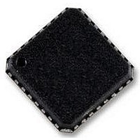
AD5748ACPZ Analog Devices Inc, AD5748ACPZ Datasheet - Page 25

AD5748ACPZ
Manufacturer Part Number
AD5748ACPZ
Description
ZDPLC +/-24V DRIVER
Manufacturer
Analog Devices Inc
Datasheet
1.AD5748ACPZ-RL7.pdf
(32 pages)
Specifications of AD5748ACPZ
Amplifier Type
Instrumentation
Number Of Circuits
1
Slew Rate
2 V/µs
Current - Output / Channel
15mA
Voltage - Supply, Single/dual (±)
±12 V ~ 24 V
Operating Temperature
-40°C ~ 105°C
Mounting Type
Surface Mount
Package / Case
*
No. Of Amplifiers
3
Supply Voltage Range
± 12V To ± 24V
Supply Current
5.2mA
Amplifier Case Style
LFCSP
No. Of Pins
32
Operating Temperature Range
-40°C To +105°C
Svhc
No
Rohs Compliant
Yes
Bandwidth
100kHz
Amplifier Output
Differential
Lead Free Status / RoHS Status
Lead free / RoHS Compliant
Output Type
-
Gain Bandwidth Product
-
-3db Bandwidth
-
Current - Input Bias
-
Voltage - Input Offset
-
Current - Supply
-
Lead Free Status / RoHS Status
Lead free / RoHS Compliant
DEFAULT REGISTERS AT POWER-ON
The AD5748 power-on reset circuit ensures that all registers are
loaded with zero code.
In software SPI mode, the part powers up with all outputs dis-
abled (OUTEN bit = 0). The user must set the OUTEN bit in
the control register to enable the output and, in the same write,
set the output range configuration using the R3 to R0 bits.
If hardware mode is selected, the part powers up to the
conditions defined by the R3 to R0 bits and the status of the
OUTEN pin. It is recommended to keep the output disabled
when powering up the part in hardware mode.
RESET FUNCTION
In software mode, the part can be reset using the RESET pin
(active low) or the reset bit (reset = 1). A reset disables both the
current and voltage outputs to their power-on condition. The
user must write to the OUTEN bit to enable the output and, in
the same write, set the output range configuration. The RESET
pin is a level-sensitive input; the part stays in reset mode as long
as the RESET pin is low. The reset bit clears to 0 following a
reset command to the control register.
In hardware mode, there is no reset. If using the part in hardware
mode, the RESET pin should be tied high.
OUTEN
In software mode, the output can be enabled or disabled using
the OUTEN bit in the control register. When the output is
Table 6. Input Shift Register Contents for a Write Operation—Control Register
MSB
D15
A2
Table 7. Input Shift Register Descriptions
Bit
A2, A1, A0
R/W
D14
A1
Description
Used in association with the AD2, AD1, and AD0 external pins to determine which part is being addressed by the system
controller
A2
0
0
0
0
1
1
1
1
Indicates a read from or a write to the addressed register
D13
A0
A1
0
0
1
1
0
0
1
1
D12
R/W
A0
0
1
0
1
0
1
0
1
D11
0
D10
R3
Function
Addresses part with Pin AD2 = 0, Pin AD1 = 0, Pin AD0 = 0
Addresses part with Pin AD2 = 0, Pin AD1 = 0, Pin AD0 = 1
Addresses part with Pin AD2 = 0, Pin AD1 = 1, Pin AD0 = 0
Addresses part with Pin AD2 = 0, Pin AD1 = 1, Pin AD0 = 1
Addresses part with Pin AD2 = 1, Pin AD1 = 0, Pin AD0 = 0
Addresses part with Pin AD2 = 1, Pin AD1 = 0, Pin AD0 = 1
Addresses part with Pin AD2 = 1, Pin AD1 = 1, Pin AD0 = 0
Addresses part with Pin AD2 = 1, Pin AD1 = 1, Pin AD0 = 1
D9
R2
D8
R1
Rev. A | Page 25 of 32
D7
R0
D6
CLRSEL
disabled, both the current and voltage channels go into tristate.
The user must set the OUTEN bit to enable the output and
simultaneously set the output range configuration.
In hardware mode, the output can be enabled or disabled using
the OUTEN pin. When the output is disabled, both the current
and voltage channels both go into tristate. The user must write
to the OUTEN pin to enable the output. It is recommended
that the output be disabled when changing the ranges.
SOFTWARE CONTROL
Software control is enabled by connecting the HW SELECT pin
to ground. In software mode, the AD5748 is controlled over a
versatile 3-wire serial interface that operates at clock rates of up
to 50 MHz. It is compatible with SPI, QSPI™, MICROWIRE,
and DSP standards.
Input Shift Register
The input shift register is 16 bits wide. Data is loaded into the
device MSB first as a 16-bit word under the control of a serial
clock input, SCLK. Data is clocked in on the falling edge of
SCLK. The input shift register consists of 16 control bits, as
shown in Table 6. The timing diagram for this write operation
is shown in Figure 2. The first three bits of the input shift register
are used to set the hardware address of the AD5748 device on
the printed circuit board (PCB). Up to eight devices can be
addressed per board.
Bit D11, Bit D1, and Bit D0 must always be set to 0 during any
write sequence.
D5
OUTEN
D4
Clear
D3
RSET
D2
Reset
AD5748
D1
0
LSB
D0
0


