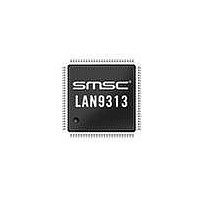
LAN9313-NZW SMSC, LAN9313-NZW Datasheet - Page 121

LAN9313-NZW
Manufacturer Part Number
LAN9313-NZW
Description
Ethernet ICs Three Port 10/100 Ethernet Switch
Manufacturer
SMSC
Type
Three Port Managed Ethernet Switchr
Datasheet
1.LAN9313-NZW.pdf
(399 pages)
Specifications of LAN9313-NZW
Ethernet Connection Type
10 Base-T, 100 Base-TX
Minimum Operating Temperature
0 C
Mounting Style
SMD/SMT
Product
Ethernet Switches
Number Of Transceivers
1
Standard Supported
802.3, 802.3u
Data Rate
10 Mbps, 100 Mbps
Supply Voltage (max)
3.6 V
Supply Voltage (min)
0 V
Supply Current (max)
155 mA, 270 mA
Maximum Operating Temperature
+ 70 C
Package / Case
TQFP-100
Lead Free Status / RoHS Status
Lead free / RoHS Compliant
Available stocks
Company
Part Number
Manufacturer
Quantity
Price
Company:
Part Number:
LAN9313-NZW
Manufacturer:
Microchip Technology
Quantity:
10 000
Part Number:
LAN9313-NZW
Manufacturer:
SMSC
Quantity:
20 000
- Current page: 121 of 399
- Download datasheet (5Mb)
Three Port 10/100 Managed Ethernet Switch with MII
Datasheet
SMSC LAN9313/LAN9313i
SCK (active high)
8.5
8.5.1
SCK (active low)
nSCS
SO
SCK (active high)
SI
SCK (active low)
Figure 8.2
When in MAC/PHY I
LAN9313/LAN9313i. All system CSRs are accessible to the CPU in these modes. I
when the mngt_mode_strap[1:0] inputs are set to 10b. The I
level I
and acknowledge generation and reception), handles the slave command protocol, and performs
system register reads and writes. The I
Specification .
The I
is driven by the master, while the data wire is bi-directional. Both signals are open-drain and require
external pull-up resistors. Both signals include Schmitt trigger inputs and digital input filters. The digital
filters reject pulses that are less than 100nS.
The I
speed of 400KHz. Refer to the Philips I
I
The I
A read or write command is started by the master first sending a start condition, followed by a control
byte. The control byte consists of a 7-bit slave address and a 1-bit read/write indication (R/~W). The
slave address used by the LAN9313/LAN9313i is 0001010b, written as SA6 (first bit on the wire)
through SA0 (last bit on the wire). Assuming the slave address in the control byte matches this
address, the control byte is acknowledged by the LAN9313/LAN9313i. Otherwise, the entire sequence
is ignored until the next start condition. The I
If the read/write indication (R/~W) in the control byte is a 0 (indicating a potential write), the next byte
sent by the master is the register address. After the address byte is acknowledged by the
I
X
X
2
2
X
C Slave Command Format
C Slave Operation
1
0
1
2
2
2
nSCS
2
C slave serial interface consists of a data wire (SDA) and a serial clock (SCL). The serial clock
C slave serial interface supports single register and multiple register read and write commands.
C slave serial interface supports the standard-mode speed of up to 100KHz and the fast-mode
2
C slave serial interface (start and stop condition detection, data bit transmission and reception,
0
SO
2
SI
3
illustrates a typical single and multiple register write.
0
3
X
X
Instruction
X
4
0
4
1
0
5
1
dec
5
2
0
6
2
inc
6
2
3
C managed mode, the I
0
7
3
1
Instruction
7
4
0
8
4
1
8
5
0
9
5
A9
9
6
0
1
0
6
A8
Figure 8.2 SPI Writes
1
0
7
1
1
1
7
A7
DATASHEET
1
1
8
Multiple Register Writes
1
Single Register Write
1
2
Address
8
A6
1
2
9
2
A9
1
3
C-Bus Specification for detailed I
9
A5
1
3
121
1
0
A8
1
4
1
0
A4
2
1
4
2
1
1
C slave controller conforms to the Philips I
A7
2
C command format can be seen in
1
5
1
1
C slave interface is used for CPU management of the
A3
1
5
1
2
Address
A6
1
6
1
2
Z
A2
1
6
Z
1
3
A5
1
7
1
3
31
D
1
7
1
4
Data 1...
A4
1
8
1
4
30
D
1
8
1
5
A3
1
9
1
5
.. .
29
D
1
9
1
6
.. .
A2
.. .
2
1
6
C slave controller implements the low
1
7
31
D
1
7
...Data m
1
8
D2
30
D
1
8
1
9
D1
.. .
29
D
1
9
.. .
D0
.. .
Data
2
4
5
C timing information.
4
5
31
D
...Data m+1
4
6
D2
4
6
30
D
4
7
Revision 1.7 (06-29-10)
D1
2
4
7
Figure
29
.. .
D
C mode is selected
4
8
.. .
D0
.. .
4
8
X
X
X
...Data n
8.3.
D2
D1
2
C-Bus
D0
X
X
X
Related parts for LAN9313-NZW
Image
Part Number
Description
Manufacturer
Datasheet
Request
R

Part Number:
Description:
Ethernet ICs Three Port 10/100 Ethernet Switch
Manufacturer:
SMSC
Datasheet:

Part Number:
Description:
FAST ETHERNET PHYSICAL LAYER DEVICE
Manufacturer:
SMSC Corporation
Datasheet:

Part Number:
Description:
357-036-542-201 CARDEDGE 36POS DL .156 BLK LOPRO
Manufacturer:
SMSC Corporation
Datasheet:

Part Number:
Description:
357-036-542-201 CARDEDGE 36POS DL .156 BLK LOPRO
Manufacturer:
SMSC Corporation
Datasheet:

Part Number:
Description:
357-036-542-201 CARDEDGE 36POS DL .156 BLK LOPRO
Manufacturer:
SMSC Corporation
Datasheet:

Part Number:
Description:
4-PORT USB2.0 HUB CONTROLLER
Manufacturer:
SMSC Corporation
Datasheet:

Part Number:
Description:
Manufacturer:
SMSC Corporation
Datasheet:

Part Number:
Description:
Manufacturer:
SMSC Corporation
Datasheet:

Part Number:
Description:
FDC37C672ENHANCED SUPER I/O CONTROLLER WITH FAST IR
Manufacturer:
SMSC Corporation
Datasheet:

Part Number:
Description:
COM90C66LJPARCNET Controller/Transceiver with AT Interface and On-Chip RAM
Manufacturer:
SMSC Corporation
Datasheet:

Part Number:
Description:
Manufacturer:
SMSC Corporation
Datasheet:

Part Number:
Description:
Manufacturer:
SMSC Corporation
Datasheet:

Part Number:
Description:
Manufacturer:
SMSC Corporation
Datasheet:

Part Number:
Description:
Manufacturer:
SMSC Corporation
Datasheet:


