NTHC5513T1G ON Semiconductor, NTHC5513T1G Datasheet - Page 2
NTHC5513T1G
Manufacturer Part Number
NTHC5513T1G
Description
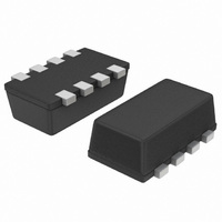
MOSFET N/P-CH 20V 2.1A CHIPFET
Manufacturer
ON Semiconductor
Datasheet
1.NTHC5513T1G.pdf
(10 pages)
Specifications of NTHC5513T1G
Fet Type
N and P-Channel
Fet Feature
Logic Level Gate
Rds On (max) @ Id, Vgs
80 mOhm @ 2.9A, 4.5V
Drain To Source Voltage (vdss)
20V
Current - Continuous Drain (id) @ 25° C
2.9A, 2.2A
Vgs(th) (max) @ Id
1.2V @ 250µA
Gate Charge (qg) @ Vgs
4nC @ 4.5V
Input Capacitance (ciss) @ Vds
180pF @ 10V
Power - Max
1.1W
Mounting Type
Surface Mount
Package / Case
8-ChipFET™
Lead Free Status / RoHS Status
Lead free / RoHS Compliant
Other names
NTHC5513T1GOS
NTHC5513T1GOS
NTHC5513T1GOSTR
NTHC5513T1GOS
NTHC5513T1GOSTR
Available stocks
Company
Part Number
Manufacturer
Quantity
Price
Company:

Part Number:
NTHC5513T1G
Manufacturer:
ON Semiconductor
Quantity:
2 200
Company:
Part Number:
NTHC5513T1G
Manufacturer:
ON
Quantity:
56 000
Part Number:
NTHC5513T1G
Manufacturer:
ON/安森美
Quantity:
20 000


2. Surface Mounted on FR4 board using 1 in sq pad size (Cu area = 1.127 in sq [1 oz] including traces).
3. Pulse Test: Pulse Width v 250 ms, Duty Cycle v 2%.
THERMAL RESISTANCE RATINGS
ELECTRICAL CHARACTERISTICS
OFF CHARACTERISTICS (Note 3)
ON CHARACTERISTICS (Note 3)
CHARGES AND CAPACITANCES
Junction−to−Ambient (Note 1)
Drain−to−Source Breakdown Voltage
Zero Gate Voltage Drain Current
Gate−to−Source Leakage Current
Gate Threshold Voltage
Drain−to−Source On Resistance
Forward Transconductance
Input Capacitance
Output Capacitance
Reverse Transfer Capacitance
Total Gate Charge
Gate−to−Source Gate Charge
Gate−to−Drain “Miller” Charge
Parameter
Parameter
(T
J
V
Symbol
R
V
Q
= 25 C unless otherwise noted)
(BR)DSS
(
C
C
GS(TH)
DS
I
I
C
G(TOT)
Q
Q
g
DSS
GSS
OSS
RSS
(
FS
ISS
GS
GD
)
(on)
Steady State
(
)
)
t v 5
N/P
http://onsemi.com
N
P
N
P
N
P
N
P
N
P
N
P
N
P
N
P
N
P
N
P
N
P
N
P
N
P
NTHC5513
T = 25 C
T
V
V
V
f = 1 MHz V
f = 1 MHz, V
A
GS
GS
GS
V
V
V
V
V
2
= 25 C
GS
GS
GS
GS
GS
= −4.5 V, V
= −4.5 V, V
= −4.5 V, V
V
V
V
V
V
= 0 V, V
V
V
= 4.5 V, V
= 4.5 V, V
= 4.5 V, V
V
GS
= 0 V, V
GS
V
V
V
GS
V
GS
DS
DS
V
GS
GS
GS
GS
DS
= V
= 0 V
= 0 V
Test Conditions
= −4.5 V , I
= −10 V , I
= −2.5 V, I
= 0 V, V
= 0 V, V
V
= 4.5 V , I
= 2.5 V , I
= 0 V, V
GS
= 10 V, I
DS
DS
DS
DS
DS
DS
= 0 V
= 0 V
DS
DS
DS
= −16 V, T
Symbol
= 16 V, T
= −10 V, I
= −10 V, I
= −10 V, I
R
= 10 V, I
= 10 V, I
= 10 V, I
DS
DS
GS
qJA
D
D
D
D
D
D
= −16 V
= −1.7 A
= 2.9A
= −2.2 A
= 16 V
= −2.2 A
= 2.3 A
= 12 V
= 2.9 A
I
I
V
V
V
J
I
D
I
D
J
V
V
V
D
D
D
D
D
D
D
D
DS
DS
DS
= 85 C
DS
DS
DS
= −250 mA
= 85 C
= −250 mA
= 2.9 A
= 2.9 A
= 2.9 A
= 250 mA
= 250 mA
= −2.2 A
= −2.2 A
= −2.2 A
= −10 V
= −10 V
= −10 V
= 10 V
= 10 V
= 10 V
Max
110
60
−0.6
Min
−20
0.6
20
0.058 0.080
0.130 0.155
0.077 0.115
0.200 0.240
Typ
180
185
6.0
6.0
2.6
3.0
0.6
0.5
0.7
0.9
80
95
25
30
Max
−1.0
−1.2
1.0
1.2
4.0
6.0
−5
100
Unit
5
C/W
Unit
nC
mA
nA
pF
W
W
V
V
S
Related parts for NTHC5513T1G
Image
Part Number
Description
Manufacturer
Datasheet
Request
R

Part Number:
Description:
ON Semiconductor [VOLTAGE REGULATOR]
Manufacturer:
ON Semiconductor
Datasheet:
Part Number:
Description:
357-036-542-201 CARDEDGE 36POS DL .156 BLK LOPRO
Manufacturer:
ON Semiconductor
Datasheet:
Part Number:
Description:
357-036-542-201 CARDEDGE 36POS DL .156 BLK LOPRO
Manufacturer:
ON Semiconductor
Datasheet:
Part Number:
Description:
357-036-542-201 CARDEDGE 36POS DL .156 BLK LOPRO
Manufacturer:
ON Semiconductor
Datasheet:
Part Number:
Description:
357-036-542-201 CARDEDGE 36POS DL .156 BLK LOPRO
Manufacturer:
ON Semiconductor
Datasheet:
Part Number:
Description:
357-036-542-201 CARDEDGE 36POS DL .156 BLK LOPRO
Manufacturer:
ON Semiconductor
Datasheet:
Part Number:
Description:
357-036-542-201 CARDEDGE 36POS DL .156 BLK LOPRO
Manufacturer:
ON Semiconductor
Datasheet:
Part Number:
Description:
357-036-542-201 CARDEDGE 36POS DL .156 BLK LOPRO
Manufacturer:
ON Semiconductor
Datasheet:
Part Number:
Description:
357-036-542-201 CARDEDGE 36POS DL .156 BLK LOPRO
Manufacturer:
ON Semiconductor
Datasheet:
Part Number:
Description:
357-036-542-201 CARDEDGE 36POS DL .156 BLK LOPRO
Manufacturer:
ON Semiconductor
Datasheet:
Part Number:
Description:
357-036-542-201 CARDEDGE 36POS DL .156 BLK LOPRO
Manufacturer:
ON Semiconductor
Datasheet:
Part Number:
Description:
Manufacturer:
ON Semiconductor
Datasheet:
Part Number:
Description:
Manufacturer:
ON Semiconductor
Datasheet:
Part Number:
Description:
Manufacturer:
ON Semiconductor
Datasheet: