CYII4SM6600AB-QDC Cypress Semiconductor Corp, CYII4SM6600AB-QDC Datasheet - Page 5
CYII4SM6600AB-QDC
Manufacturer Part Number
CYII4SM6600AB-QDC
Description
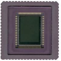
SENSOR IMAGE MONO CMOS 68-LCC
Manufacturer
Cypress Semiconductor Corp
Type
CMOS Imagingr
Datasheet
1.CYII4SC6600-EVAL.pdf
(34 pages)
Specifications of CYII4SM6600AB-QDC
Package / Case
68-LCC
Pixel Size
3.5µm x 3.5µm
Active Pixel Array
2210H x 3002V
Frames Per Second
5
Voltage - Supply
2.5V, 3.3V
Operating Supply Voltage
2.5 V to 3.3 V
Maximum Operating Temperature
+ 65 C
Minimum Operating Temperature
- 30 C
Image Size
2210 H x 3002 V
Color Sensing
Black/White
Sensor Image Color Type
Monochrome
Sensor Image Size Range
>= 480,000Pixels
Sensor Image Size
2210x3002Pixels
Operating Supply Voltage (min)
2.5V
Operating Supply Voltage (typ)
2.5V
Operating Supply Voltage (max)
3.3V
Operating Temp Range
-30C to 65C
Package Type
CLCC
Operating Temperature Classification
Commercial
Mounting
Surface Mount
Pin Count
68
Package
68CLCC
Operating Temperature
-30 to 65 °C
Lead Free Status / RoHS Status
Contains lead / RoHS non-compliant
Lead Free Status / RoHS Status
Lead free / RoHS Compliant, Contains lead / RoHS non-compliant


Electrical Specifications
Absolute Maximum Ratings
Exceeding maximum ratings may shorten the useful life of the device. User guidelines are not tested. Stresses beyond those listed
under
at these or any other conditions beyond those indicated in the operational sections are not implied.
Table 2. Absolute Maximum Ratings
Recommended Operating Conditions
All parameters are characterized for DC conditions after thermal equilibrium is established. Unused inputs must always be tied to an
appropriate logic level, for example, V
This device contains circuitry to protect the inputs against damage caused by high static voltages or electric fields. However, you must
take normal precautions to avoid applying voltages higher than the maximum rated voltages to this high impedance circuit.
DC Electrical Conditions
Note
Document Number: 001-02366 Rev. *G
1. V
V
V
V
I
T
T
H
ESD
V
T
V
V
I
V
V
I
IO
IN
DD
A
DD
IN
OUT
L
ST
DD
IH
IL
OH
OL
DD
Symbol
Symbol
Symbol
[1]
Table 2
= V
DDD
= V
may cause permanent damage to the device. These are stress ratings only and the functional operation of the device
DDA
DC Supply Voltage
DC Input Voltage
DC Output Voltage
DC Current Drain Per Pin; Any Single Input or Output
Lead Temperature (5 seconds soldering)
Storage Temperature
Humidity (Relative)
ESD Susceptibility
DC Supply Voltage
Commercial Operating Temperature
Input High Voltage
Input Low Voltage
Input Leakage Current
Output High Voltage
Output Low Voltage
Operating Current
(V
DDD
Characteristic
is supply to digital circuit, V
DD
Parameter
Parameter
or GND.
V
V
V
System clock <= 40 MHz
DDA
IN
DD
DD
to analog circuit).
= V
=min; I
=min; I
DD
Condition
or GND
OH
OH
= –100 mA
= 100 mA
Min
–30
V
V
2.5
DD
DD
–0.6
Min
–10
70
–0.5 to (V
–0.5 to (V
-0.5
-0.5
85% at 85 °C
IBIS4-6600 CYII4SM6600AB
–0.5 to 3.3
–30 to +85
Value
2000
± 50
350
Typ
2.5
24
DD
DD
+ 0.5)
+ 0.5)
Max
+10
0.6
0.5
80
Max
+65
3.3
Unit
Unit
Unit
mA
mA
°C
°C
°C
µA
V
V
V
V
V
V
V
V
V
Page 5 of 34
[+] Feedback
Related parts for CYII4SM6600AB-QDC
Image
Part Number
Description
Manufacturer
Datasheet
Request
R

Part Number:
Description:
Manufacturer:
Cypress Semiconductor Corp
Datasheet:
Part Number:
Description:
Manufacturer:
Cypress Semiconductor Corp
Datasheet:
Part Number:
Description:
Manufacturer:
Cypress Semiconductor Corp
Datasheet:
Part Number:
Description:
Manufacturer:
Cypress Semiconductor Corp
Datasheet:
Part Number:
Description:
Manufacturer:
Cypress Semiconductor Corp
Datasheet: