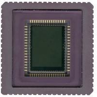
CYII4SM6600AB-QDC Cypress Semiconductor Corp, CYII4SM6600AB-QDC Datasheet - Page 26

CYII4SM6600AB-QDC
Manufacturer Part Number
CYII4SM6600AB-QDC
Description
SENSOR IMAGE MONO CMOS 68-LCC
Manufacturer
Cypress Semiconductor Corp
Type
CMOS Imagingr
Datasheet
1.CYII4SC6600-EVAL.pdf
(34 pages)
Specifications of CYII4SM6600AB-QDC
Package / Case
68-LCC
Pixel Size
3.5µm x 3.5µm
Active Pixel Array
2210H x 3002V
Frames Per Second
5
Voltage - Supply
2.5V, 3.3V
Operating Supply Voltage
2.5 V to 3.3 V
Maximum Operating Temperature
+ 65 C
Minimum Operating Temperature
- 30 C
Image Size
2210 H x 3002 V
Color Sensing
Black/White
Sensor Image Color Type
Monochrome
Sensor Image Size Range
>= 480,000Pixels
Sensor Image Size
2210x3002Pixels
Operating Supply Voltage (min)
2.5V
Operating Supply Voltage (typ)
2.5V
Operating Supply Voltage (max)
3.3V
Operating Temp Range
-30C to 65C
Package Type
CLCC
Operating Temperature Classification
Commercial
Mounting
Surface Mount
Pin Count
68
Package
68CLCC
Operating Temperature
-30 to 65 °C
Lead Free Status / RoHS Status
Contains lead / RoHS non-compliant
Lead Free Status / RoHS Status
Lead free / RoHS Compliant, Contains lead / RoHS non-compliant
ADC Timing
Two Analog Outputs
Figure 26
(in case of internal clock, the clock is half the SYS_CLOCK).
T1: Each ADC has a pipeline delay of 2 ADC_CLOCK cycles. This results in a total pipeline delay of four pixels.
One Analog Output
Figure 27
T1: The ADC has a pipeline delay of 2 ADC_CLOCK cycles.
Document Number: 001-02366 Rev. *G
shows the timing of the ADC using two analog outputs. Internally, the ADCs sample on the falling edge of the ADC_CLOCK
shows the timing of the ADC using one analog output. Internally, the ADC samples on the falling edge of the ADC_CLOCK.
Figure 26. ADC Timing using Two Analog Outputs
Figure 27. ADC Timing using One Analog Output
IBIS4-6600 CYII4SM6600AB
Page 26 of 34
[+] Feedback


