CYII4SM6600AB-QDC Cypress Semiconductor Corp, CYII4SM6600AB-QDC Datasheet - Page 23
CYII4SM6600AB-QDC
Manufacturer Part Number
CYII4SM6600AB-QDC
Description
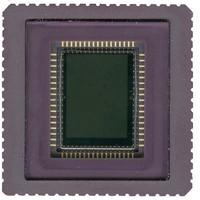
SENSOR IMAGE MONO CMOS 68-LCC
Manufacturer
Cypress Semiconductor Corp
Type
CMOS Imagingr
Datasheet
1.CYII4SC6600-EVAL.pdf
(34 pages)
Specifications of CYII4SM6600AB-QDC
Package / Case
68-LCC
Pixel Size
3.5µm x 3.5µm
Active Pixel Array
2210H x 3002V
Frames Per Second
5
Voltage - Supply
2.5V, 3.3V
Operating Supply Voltage
2.5 V to 3.3 V
Maximum Operating Temperature
+ 65 C
Minimum Operating Temperature
- 30 C
Image Size
2210 H x 3002 V
Color Sensing
Black/White
Sensor Image Color Type
Monochrome
Sensor Image Size Range
>= 480,000Pixels
Sensor Image Size
2210x3002Pixels
Operating Supply Voltage (min)
2.5V
Operating Supply Voltage (typ)
2.5V
Operating Supply Voltage (max)
3.3V
Operating Temp Range
-30C to 65C
Package Type
CLCC
Operating Temperature Classification
Commercial
Mounting
Surface Mount
Pin Count
68
Package
68CLCC
Operating Temperature
-30 to 65 °C
Lead Free Status / RoHS Status
Contains lead / RoHS non-compliant
Lead Free Status / RoHS Status
Lead free / RoHS Compliant, Contains lead / RoHS non-compliant


Serial to Parallel Interface
To upload the sequencer registers, a dedicated serial to parallel interface (SPI) is implemented. 16 bits (4 address bits + 12 data bits)
must be uploaded serially. The address must be uploaded first (MSB first), then the data (also MSB first).
The elementary unit cell is shown in
entire uploadable parameter block. Dout of one cell is connected to SPI_DATA of the next cell (maximum speed is 20 MHz). The
uploaded settings on the address/data bus are loaded into the correct register of the sensor on the rising edge of signal REG_CLOCK
and become effective immediately.
Timing Diagrams
Sequencer Control Signals
There are 3 control signals that operate the image sensor:
■
■
■
Document Number: 001-02366 Rev. *G
SYS_CLOCK
Y_CLOCK
Y_START
REG_CLOCK
SPI_DATA
SPI_CLK
Unity C ell
D
D
C
C
Q
Q
To address/data bus
Figure 22. Relative Timing of the Three Control Signals
Figure
Dout
21. Sixteen of these cells are connected in series, having a common SPI_CLK form the
SPI_DATA
SPI_CLK
Figure 21. SPI Interface
REG_CLOCK
SPI_DATA
SPI_CLK
REG_CLOCK
These control signals must be generated by the external system
with the following time constraints to SYS_CLOCK
(rising edge = active edge):
■
■
It is important that these signals are free of any glitches.
TSETUP >7.5 ns
THOLD > 7.5 ns
A3
16 outputs to address/data bus
E ntire uploadable addres s block
A2
IBIS4-6600 CYII4SM6600AB
A1
D0
Internal register
upload
Page 23 of 34
[+] Feedback
Related parts for CYII4SM6600AB-QDC
Image
Part Number
Description
Manufacturer
Datasheet
Request
R

Part Number:
Description:
Manufacturer:
Cypress Semiconductor Corp
Datasheet:
Part Number:
Description:
Manufacturer:
Cypress Semiconductor Corp
Datasheet:
Part Number:
Description:
Manufacturer:
Cypress Semiconductor Corp
Datasheet:
Part Number:
Description:
Manufacturer:
Cypress Semiconductor Corp
Datasheet:
Part Number:
Description:
Manufacturer:
Cypress Semiconductor Corp
Datasheet: