ADAU1445YSVZ-3A-RL Analog Devices Inc, ADAU1445YSVZ-3A-RL Datasheet - Page 6
ADAU1445YSVZ-3A-RL
Manufacturer Part Number
ADAU1445YSVZ-3A-RL
Description
175MHZ SigmaDSP,2x8 SRCs
Manufacturer
Analog Devices Inc
Series
SigmaDSP®r
Type
Audio Processorr
Specifications of ADAU1445YSVZ-3A-RL
Applications
Automotive Audio
Mounting Type
Surface Mount
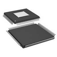
Package / Case
100-TQFP Exposed Pad, 100-eTQFP, 100-HTQFP, 100-VQFP
Format
Fixed Point
Program Memory Size
Not RequiredKB
Operating Supply Voltage (typ)
1.8/3.3V
Operating Temp Range
-40C to 105C
Operating Temperature Classification
Industrial
Mounting
Surface Mount
Pin Count
100
Lead Free Status / RoHS Status
Lead free / RoHS Compliant
Lead Free Status / RoHS Status
Lead free / RoHS Compliant
Available stocks
Company
Part Number
Manufacturer
Quantity
Price
Company:

Part Number:
ADAU1445YSVZ-3A-RL
Manufacturer:
Analog Devices Inc
Quantity:
10 000


ADAU1445/ADAU1446
DIGITAL TIMING SPECIFICATIONS
T
Table 2.
Parameter
MASTER CLOCK
CORE CLOCK
SERIAL PORT
SPI PORT
I
MULTIPURPOSE PINS AND RESET
1
2
2
All timing specifications are given for the default (I
Maximum SPI CCLK clock frequency is dependent on current drive strength and capacitive loads on the circuit board.
C PORT
A
f
t
t
CLKOUT Jitter
f
f
t
t
t
t
t
t
t
t
t
t
f
f
t
t
t
t
t
t
t
t
t
f
t
t
t
t
t
t
t
t
t
t
t
f
t
t
= −40°C to +105°C, DVDD = 1.8 V, IOVDD = 3.3 V.
MP
MP
MD
CORE
BCLK
BCLK
BIL
BIH
LIS
LIH
SIS
SIH
TS
SODS
SODM
CCLK write
CCLK read
CCPL
CCPH
CLS
CLH
CLPH
CLDLY
CDS
CDH
COV
SCL
SCLH
SCLL
SCS
SCH
DS
DH
SCLR
SCLF
SDR
SDF
BFT
MP
MPIL
RLPW
1
Min
2.822
40.69
25
40.69
30
30
20
20
10
10
20
20
0
35
20
20
0
35
0.6
1.3
0.6
0.6
100
0.9
1.3
10
2
S) states of the serial audio input ports and the serial audio output ports (see Table 24 and Table 28).
Max
24.576
354.36
75
250
172.032
24.576
5
30
30
32
16
40
400
300
300
300
300
f
1.5 × 1/f
S
/2
S,NORMAL
Rev. A | Page 6 of 92
Unit
MHz
ns
%
ps
MHz
MHz
ns
ns
ns
ns
ns
ns
ns
ns
ns
ns
MHz
MHz
ns
ns
ns
ns
ns
ns
ns
ns
ns
kHz
μs
μs
μs
μs
ns
μs
ns
ns
ns
ns
μs
Hz
μs
ns
Description
Master clock (MCLK) frequency. See the Master Clock and PLL section.
Master clock (MCLK) period. See the
Master clock (MCLK) duty cycle.
Cycle-to-cycle rms average.
DSP core clock frequency.
BCLK frequency.
BCLK period.
BCLKx low pulse width, slave mode.
BCLKx high pulse width, slave mode.
LRCLKx setup to BCLKx input rising edge, slave mode.
LRCLKx hold from BCLKx input rising edge, slave mode.
SDATA_INx setup to BCLKx input rising edge.
SDATA_INx hold from BCLKx input rising edge.
BCLKx output falling edge to LRCLKx output timing skew.
SDATA_OUTx delay in slave mode from BCLKx output falling edge.
SDATA_OUTx delay in master mode from BCLKx output falling edge.
CCLK pulse width low.
CCLK pulse width high.
CLATCH setup to CCLK rising edge.
CLATCH hold from CCLK rising edge.
CLATCH pulse width high.
Minimum delay between CLATCH low pulses.
CDATA setup to CCLK rising edge.
CDATA hold from CCLK rising edge.
COUT valid output delay from CCLK falling edge.
SCL clock frequency.
SCL pulse width high.
SCL pulse width low.
Start and repeated start condition setup time.
Start condition hold time.
Data setup time.
Data hold time.
SCL rise time.
SCL fall time.
SDA rise time.
SDA fall time.
Bus-free time between stop and start.
MPx maximum switching rate.
MPx pin input latency until high/low value is read by core. Guaranteed by
design.
RESET low pulse width.
CCLK frequency.
CCLK frequency.
2
2
Master Clock and PLL
section.
Related parts for ADAU1445YSVZ-3A-RL
Image
Part Number
Description
Manufacturer
Datasheet
Request
R

Part Number:
Description:
SigmaDSP� Digital Audio Processor with Flexible Audio Routing Matrix
Manufacturer:
Analog Devices
Datasheet:

Part Number:
Description:
±1.7g Dual-Axis IMEMS Accelerometer Evaluation Board
Manufacturer:
Analog Devices Inc
Datasheet:

Part Number:
Description:
Inertial Sensor Evaluation System
Manufacturer:
Analog Devices Inc
Datasheet:
Part Number:
Description:
Manufacturer:
Analog Devices Inc
Datasheet:
Part Number:
Description:
Manufacturer:
Analog Devices Inc
Datasheet:
Part Number:
Description:
Manufacturer:
Analog Devices Inc
Datasheet:
Part Number:
Description:
Manufacturer:
Analog Devices Inc
Datasheet:
Part Number:
Description:
Manufacturer:
Analog Devices Inc
Datasheet:
Part Number:
Description:
Manufacturer:
Analog Devices Inc
Datasheet:
Part Number:
Description:
Manufacturer:
Analog Devices Inc
Datasheet:
Part Number:
Description:
Manufacturer:
Analog Devices Inc
Datasheet:
Part Number:
Description:
Manufacturer:
Analog Devices Inc
Datasheet:
Part Number:
Description:
Manufacturer:
Analog Devices Inc
Datasheet: