AD9233-125EBZ Analog Devices Inc, AD9233-125EBZ Datasheet - Page 24
AD9233-125EBZ
Manufacturer Part Number
AD9233-125EBZ
Description
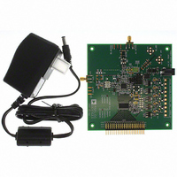
1.8V 12Bit 125 Msps ADC EB
Manufacturer
Analog Devices Inc
Datasheet
1.AD9233BCPZ-125.pdf
(44 pages)
Specifications of AD9233-125EBZ
Number Of Adc's
1
Number Of Bits
12
Sampling Rate (per Second)
125M
Data Interface
Serial
Inputs Per Adc
1 Differential
Input Range
1 ~ 2 Vpp
Power (typ) @ Conditions
455mW @125MSPS
Voltage Supply Source
Single Supply
Operating Temperature
-40°C ~ 85°C
Utilized Ic / Part
AD9233
Lead Free Status / RoHS Status
Lead free / RoHS Compliant


AD9233
MEMORY MAP
READING THE MEMORY MAP TABLE
Each row in the memory map table has eight address locations.
The memory map is roughly divided into three sections: chip
configuration registers map (Address 0x00 to Address 0x02),
device index and transfer registers map (Address 0xFF), and
ADC functions map (Address 0x08 to Address 0x18).
The memory map register in Table 15 displays the register
address number in hexadecimal in the first column. The last
column displays the default value for each hexadecimal address.
The Bit 7 (MSB) column is the start of the default hexadecimal
value given. For example, Hexadecimal Address 0x14,
output_phase has a hexadecimal default value of 0x00. This
means Bit 3 = 0, Bit 2 = 0, Bit 1 = 1, and Bit 0 = 1 or 0011 in
binary. This setting is the default output clock or DCO phase
adjust option. The default value adjusts the DCO phase 90°
relative to the nominal DCO edge and 180° relative to the data
edge. For more information on this function, consult the
Interfacing to High Speed ADCs via SPI User
Open Locations
Locations marked as open are currently not supported for this
device. When required, these locations should be written with
0s. Writing to these locations is required only when part of an
address location is open (for example, Address 0x14). If the
entire address location is open (Address 0x13), then the address
location does not need to be written.
Default Values
Coming out of reset, critical registers are loaded with default
values. The default values for the registers are provided in Table 15.
SCLK
SDIO
CSB
DON’T CARE
DON’T CARE
t
S
R/W
t
DS
W1
W0
t
DH
A12
Manual.
A11
t
HI
Figure 57. Serial Port Interface Timing Diagram
A10
t
LO
A9
Rev. A | Page 24 of 44
t
CLK
A8
A7
Logic Levels
An explanation of two registers follows:
•
•
SPI-Accessible Features
A list of features accessible via the SPI and a brief description of
what the user can do with these features follows. These features
are described in detail in the
SPI User
•
•
•
•
•
•
•
Bit is set is synonymous with bit is set to Logic 1 or writing
Logic 1 for the bit.
Clear a bit is synonymous with bit is set to Logic 0 or
writing Logic 0 for the bit.
Modes: Set either power-down or standby mode.
Clock: Access the DCS via the SPI.
Offset: Digitally adjust the converter offset.
Test I/O: Set test modes to have known data on output bits.
Output Mode: Setup outputs, vary the strength of the
output drivers.
Output Phase: Set the output clock polarity.
VREF: Set the reference voltage.
Manual.
D5
D4
D3
Interfacing to High Speed ADCs via
D2
D1
D0
t
H
DON’T CARE
DON’T CARE
Related parts for AD9233-125EBZ
Image
Part Number
Description
Manufacturer
Datasheet
Request
R

Part Number:
Description:
1.8V 12Bit 80 Msps ADC EB
Manufacturer:
Analog Devices Inc
Datasheet:

Part Number:
Description:
±1.7g Dual-Axis IMEMS Accelerometer Evaluation Board
Manufacturer:
Analog Devices Inc
Datasheet:
Part Number:
Description:
Inertial Sensor Evaluation System
Manufacturer:
Analog Devices Inc
Datasheet:
Part Number:
Description:
Manufacturer:
Analog Devices Inc
Datasheet:
Part Number:
Description:
Manufacturer:
Analog Devices Inc
Datasheet:
Part Number:
Description:
Manufacturer:
Analog Devices Inc
Datasheet:
Part Number:
Description:
Manufacturer:
Analog Devices Inc
Datasheet:
Part Number:
Description:
Manufacturer:
Analog Devices Inc
Datasheet:
Part Number:
Description:
Manufacturer:
Analog Devices Inc
Datasheet:
Part Number:
Description:
Manufacturer:
Analog Devices Inc
Datasheet:
Part Number:
Description:
Manufacturer:
Analog Devices Inc
Datasheet:
Part Number:
Description:
Manufacturer:
Analog Devices Inc
Datasheet:
Part Number:
Description:
Manufacturer:
Analog Devices Inc
Datasheet: