AD9233-125EBZ Analog Devices Inc, AD9233-125EBZ Datasheet - Page 19
AD9233-125EBZ
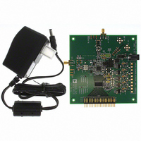
Manufacturer Part Number
AD9233-125EBZ
Description
1.8V 12Bit 125 Msps ADC EB
Manufacturer
Analog Devices Inc
Datasheet
1.AD9233BCPZ-125.pdf
(44 pages)
Specifications of AD9233-125EBZ
Number Of Adc's
1
Number Of Bits
12
Sampling Rate (per Second)
125M
Data Interface
Serial
Inputs Per Adc
1 Differential
Input Range
1 ~ 2 Vpp
Power (typ) @ Conditions
455mW @125MSPS
Voltage Supply Source
Single Supply
Operating Temperature
-40°C ~ 85°C
Utilized Ic / Part
AD9233
Lead Free Status / RoHS Status
Lead free / RoHS Compliant


CLOCK
A third option is to ac-couple a differential LVDS signal to the
sample clock input pins, as shown in Figure 48. The AD9510/
AD9511/AD9512/AD9513/AD9514/AD9515
drivers offers excellent jitter performance.
CLOCK
CLOCK
In some applications, it is acceptable to drive the sample clock
inputs with a single-ended CMOS signal. In such applications,
directly drive CLK+ from a CMOS gate, while bypassing the
CLK− pin to ground with a 0.1 μF capacitor. Although the
CLK+ input circuit supply is AVDD (1.8 V), this input is
designed to withstand input voltages up to 3.6 V, making the
selection of the drive logic voltage very flexible. When driving
CLK+ with a 1.8 V CMOS signal, it is required to bias the
CLK− pin with a 0.1 μF capacitor in parallel with a 39 kΩ
resistor (see Figure 49). The 39 kΩ resistor is not required when
driving CLK+ with a 3.3 V CMOS signal (see Figure 50).
CLOCK
Clock Duty Cycle
Typical high speed ADCs use both clock edges to generate a
variety of internal timing signals. As a result, these ADCs may
be sensitive to clock duty cycle. Commonly, a ±5% tolerance is
required on the clock duty cycle to maintain dynamic perform-
ance characteristics.
The AD9233 contains a DCS that retimes the nonsampling, or
falling edge, providing an internal clock signal with a nominal
50% duty cycle. This allows a wide range of clock input duty
cycles without affecting the performance of the AD9233. Noise
INPUT
INPUT
INPUT
INPUT
50Ω*
*50Ω RESISTORS ARE OPTIONAL
*50Ω RESISTOR IS OPTIONAL
50Ω*
*50Ω RESISTOR IS OPTIONAL
50Ω*
Figure 49. Single-Ended 1.8 V CMOS Sample Clock
Figure 50. Single-Ended 3.3 V CMOS Sample Clock
0.1µF
0.1µF
50Ω*
Figure 48. Differential LVDS Sample Clock
0.1µF
0.1µF
VCC
VCC
1kΩ
1kΩ
1kΩ
1kΩ
CLK
CLK
LVDS DRIVER
AD951x
CMOS DRIVER
CMOS DRIVER
AD951x
AD951x
0.1µF
OPTIONAL
OPTIONAL
100Ω
100Ω
100Ω
0.1µF
0.1µF
39kΩ
0.1µF
0.1µF
0.1µF
family of clock
CLK+
CLK–
CLK+
CLK–
CLK+
CLK–
AD9233
AD9233
AD9233
ADC
ADC
ADC
Rev. A | Page 19 of 44
and distortion performance are nearly flat for a wide range of
duty cycles when the DCS is on, as shown in Figure 31.
Jitter in the rising edge of the input is still of paramount
concern and is not reduced by the internal stabilization circuit.
The duty cycle control loop does not function for clock rates
less than 20 MHz nominally. The loop has a time constant
associated with it that needs to be considered in applications
where the clock rate can change dynamically, which requires a
wait time of 1.5 μs to 5 μs after a dynamic clock frequency
increase (or decrease) before the DCS loop is relocked to the
input signal. During the time the loop is not locked, the DCS
loop is bypassed, and the internal device timing is dependant
on the duty cycle of the input clock signal. In such an application,
it can be appropriate to disable the duty cycle stabilizer. In all
other applications, enabling the DCS circuit is recommended to
maximize ac performance.
The DCS can be enabled or disabled by setting the SDIO/DCS
pin when operating in the external pin mode (see Table 10), or
via the SPI, as described in the Table 15.
Table 10. Mode Selection (External Pin Mode)
Voltage at Pin
AGND
AVDD
JITTER CONSIDERATIONS
High speed, high resolution ADCs are sensitive to the quality of
the clock input. The degradation in SNR at a given input
frequency (F
In the equation, the rms aperture jitter (t
mean-square of all jitter sources, which include the clock input,
analog input signal, and ADC aperture jitter specification. IF
undersampling applications are particularly sensitive to jitter, as
shown in Figure 51.
SNR = −20 log (2π × F
70
65
60
55
50
45
40
1
IN
Figure 51. SNR vs. Input Frequency and Jitter
) due to jitter (t
PERFORMANCE
SCLK/DFS
Binary (default)
Twos complement
MEASURED
INPUT FREQUENCY (MHz)
10
IN
× t
J
) is calculated as
J
)
J
SDIO/DCS
DCS disabled
DCS enabled (default)
) represents the root-
100
0.05ps
0.20ps
0.5ps
1.0ps
1.50ps
2.00ps
2.50ps
3.00ps
AD9233
1000
Related parts for AD9233-125EBZ
Image
Part Number
Description
Manufacturer
Datasheet
Request
R

Part Number:
Description:
1.8V 12Bit 80 Msps ADC EB
Manufacturer:
Analog Devices Inc
Datasheet:

Part Number:
Description:
±1.7g Dual-Axis IMEMS Accelerometer Evaluation Board
Manufacturer:
Analog Devices Inc
Datasheet:
Part Number:
Description:
Inertial Sensor Evaluation System
Manufacturer:
Analog Devices Inc
Datasheet:
Part Number:
Description:
Manufacturer:
Analog Devices Inc
Datasheet:
Part Number:
Description:
Manufacturer:
Analog Devices Inc
Datasheet:
Part Number:
Description:
Manufacturer:
Analog Devices Inc
Datasheet:
Part Number:
Description:
Manufacturer:
Analog Devices Inc
Datasheet:
Part Number:
Description:
Manufacturer:
Analog Devices Inc
Datasheet:
Part Number:
Description:
Manufacturer:
Analog Devices Inc
Datasheet:
Part Number:
Description:
Manufacturer:
Analog Devices Inc
Datasheet:
Part Number:
Description:
Manufacturer:
Analog Devices Inc
Datasheet:
Part Number:
Description:
Manufacturer:
Analog Devices Inc
Datasheet:
Part Number:
Description:
Manufacturer:
Analog Devices Inc
Datasheet: