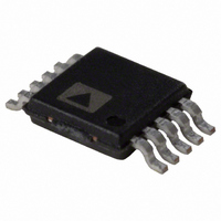
AD5426YRM Analog Devices Inc, AD5426YRM Datasheet - Page 3

AD5426YRM
Manufacturer Part Number
AD5426YRM
Description
8-IOUT DAC WITH SERIAL ITF I.C.
Manufacturer
Analog Devices Inc
Datasheet
1.AD5443YRMZ.pdf
(28 pages)
Specifications of AD5426YRM
Rohs Compliant
NO
Rohs Status
RoHS non-compliant
Design Resources
Unipolar, Precision DC Digital-to-Analog Conversion Using AD5426/32/43 8-Bit to12-Bit DACs (CN0034) Precision, Bipolar Configuration for the AD5426/32/43 8-Bit to12-Bit DACs (CN0036) AC Signal Processing Using AD5426/32/43 Current Output DACs (CN0037) Programmable Gain Element Using AD5426/32/43 Current Output DACs (CN0038)
Number Of Bits
8
Data Interface
Serial
Number Of Converters
1
Voltage Supply Source
Single Supply
Operating Temperature
-40°C ~ 125°C
Mounting Type
Surface Mount
Package / Case
10-MSOP, Micro10™, 10-uMAX, 10-uSOP
Power Dissipation (max)
25µW
Settling Time
50ns
Lead Free Status / RoHS Status
Available stocks
Company
Part Number
Manufacturer
Quantity
Price
Part Number:
AD5426YRM
Manufacturer:
ADI/亚德诺
Quantity:
20 000
Company:
Part Number:
AD5426YRMZ
Manufacturer:
MAX
Quantity:
26
Part Number:
AD5426YRMZ
Manufacturer:
ADI/亚德诺
Quantity:
20 000
SPECIFICATIONS
V
otherwise noted; dc performance measured with OP177; ac performance with AD8038, unless otherwise noted.
Table 1.
Parameter
STATIC PERFORMANCE
REFERENCE INPUT
DIGITAL INPUT/OUTPUT
DYNAMIC PERFORMANCE
DD
AD5426
AD5432
AD5443
Gain Error
Gain Error Temperature Coefficient
Output Leakage Current
Reference Input Range
V
R
Input Capacitance
Input High Voltage, V
Input Low Voltage, V
Output High Voltage, V
Output Low Voltage, V
Input Leakage Current, I
Input Capacitance
Reference Multiplying Bandwidth
Output Voltage Settling Time
Digital Delay
10% to 90% Rise/Fall Time
Digital-to-Analog Glitch Impulse
Multiplying Feedthrough Error
REF
FB
= 2.5 V to 5.5 V, V
Resolution
Relative Accuracy
Differential Nonlinearity
Resolution
Relative Accuracy
Differential Nonlinearity
Resolution
Relative Accuracy
Differential Nonlinearity
Code Zero Scale
Code Full Scale
Measured to ±16 mV of FS
Measured to ±4 mV of FS
Measured to ±1 mV of FS
Resistance
Input Resistance
1
REF
IL
IH
1
OL
OH
1
= 10 V, I
IL
OUT
1
2 = 0 V; temperature range for Y version: −40°C to +125°C; all specifications T
Min
8
8
1.7
V
V
DD
DD
− 1
− 0.5
Typ
±5
±10
10
10
3
5
4
10
50
55
90
40
15
2
70
48
Max
8
±0.25
±0.5
10
±0.5
±1
12
±1
−1/+2
±10
±10
±20
12
12
6
8
0.6
0.4
0.4
1
10
100
110
160
75
30
Rev. C | Page 3 of 28
Unit
Bits
LSB
LSB
Bits
LSB
LSB
Bits
LSB
LSB
mV
ppm FSR/°C
nA
nA
V
kΩ
kΩ
pF
pF
V
V
V
V
V
V
μA
pF
MHz
ns
ns
ns
nV-s
dB
dB
ns
ns
Conditions
Guaranteed monotonic
Guaranteed monotonic
Guaranteed monotonic
Data = 0x0000, T
Data = 0x0000, T = −40°C to 125°C, I
Input resistance TC = −50 ppm/°C
Input resistance TC = −50 ppm/°C
V
V
V
V
V
V
loaded with 0s and 1s
Interface delay time
Rise and fall time, V
1 LSB change around major carry, V
DAC latch loaded with all 0s, V
1 MHz
10 MHz
DD
DD
DD
DD
REF
REF
= 4.5 V to 5 V, I
= 2.5 V to 3.6 V, I
= 4.5 V to 5 V, I
= 2.5 V to 3.6 V, I
= ±3.5 V; DAC loaded all 1s
= 10 V; R
LOAD
AD5426/AD5432/AD5443
A
= 100 Ω, DAC latch alternately
= 25°C, I
SOURCE
SINK
REF
SOURCE
SINK
= 200 μA
= 10 V, R
= 200 μA
= 200 μA
= 200 μA
OUT
1
REF
LOAD
MIN
= ±3.5
to T
= 100 Ω
REF
OUT
= 0 V
1
MAX
, unless


