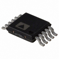
AD5426YRM Analog Devices Inc, AD5426YRM Datasheet - Page 10

AD5426YRM
Manufacturer Part Number
AD5426YRM
Description
8-IOUT DAC WITH SERIAL ITF I.C.
Manufacturer
Analog Devices Inc
Datasheet
1.AD5443YRMZ.pdf
(28 pages)
Specifications of AD5426YRM
Rohs Compliant
NO
Rohs Status
RoHS non-compliant
Design Resources
Unipolar, Precision DC Digital-to-Analog Conversion Using AD5426/32/43 8-Bit to12-Bit DACs (CN0034) Precision, Bipolar Configuration for the AD5426/32/43 8-Bit to12-Bit DACs (CN0036) AC Signal Processing Using AD5426/32/43 Current Output DACs (CN0037) Programmable Gain Element Using AD5426/32/43 Current Output DACs (CN0038)
Number Of Bits
8
Data Interface
Serial
Number Of Converters
1
Voltage Supply Source
Single Supply
Operating Temperature
-40°C ~ 125°C
Mounting Type
Surface Mount
Package / Case
10-MSOP, Micro10™, 10-uMAX, 10-uSOP
Power Dissipation (max)
25µW
Settling Time
50ns
Lead Free Status / RoHS Status
Available stocks
Company
Part Number
Manufacturer
Quantity
Price
Part Number:
AD5426YRM
Manufacturer:
ADI/亚德诺
Quantity:
20 000
Company:
Part Number:
AD5426YRMZ
Manufacturer:
MAX
Quantity:
26
Part Number:
AD5426YRMZ
Manufacturer:
ADI/亚德诺
Quantity:
20 000
AD5426/AD5432/AD5443
Figure 18. Gain and Offset Errors vs. V
–0.1
–0.2
–0.3
–0.4
–0.5
0.5
0.4
0.3
0.2
0.1
–1
–2
–3
–1
–2
–3
–4
–5
0
3
2
1
0
4
3
2
1
0
0.5
0.5
0
V
T
V
V
AD5443
T
V
T
V
V
AD5443
A
A
REF
DD
A
Figure 19. Linearity vs. V
REF
DD
Figure 20. Linearity vs. V
REF
DD
= 25°C
= 25°C
= 25°C
0.2
= 3V AND 5V
= 5V
= 5V
= 2.5V
= 0V
= 2.5V
MAX DNL
0.4
OFFSET ERROR
1.0
0.6
MIN DNL
1.0
MIN INL
0.8
V
V
V
BIAS
BIAS
BIAS
BIAS
BIAS
MAX DNL
1.0
1.5
Voltage Applied to I
Voltage Applied to I
(V)
(V)
(V)
BIAS
1.2
MAX INL
Voltage Applied to I
MIN DNL
1.5
MIN INL
1.4
2.0
GAIN ERROR
MAX INL
1.6
OUT
OUT
1.8
2
2
OUT
2.0
2.5
2.0
2
Rev. C | Page 10 of 28
Figure 21. Supply Current vs. Logic Input Voltage, SYNC (SCLK), DATA = 0
0.50
0.45
0.40
0.35
0.30
0.25
0.20
0.15
0.10
0.05
0.7
0.6
0.5
0.4
0.3
0.2
0.1
1.6
1.4
1.2
1.0
0.8
0.6
0.4
0.2
0
0
0
–40
–60
0
T
ALL 1s
A
Figure 22. I
= 25°C
–40
–20
Figure 23. Supply Current vs. Temperature
–20
1
V
0
OUT
DD
0
1 Leakage Current vs. Temperature
= 3V
V
V
DD
INPUT VOLTAGE (V)
TEMPERATURE (°C)
TEMPERATURE (°C)
20
DD
20
= 5V
2
= 3V
ALL 0s
40
40
V
I
DD
OUT
60
60
3
= 5V
1 V
I
DD
OUT
80
80
ALL 0s
ALL 1s
3V
1 V
100
DD
4
100
5V
120
120
140
5


