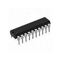
DAC0832LCN National Semiconductor, DAC0832LCN Datasheet - Page 4

DAC0832LCN
Manufacturer Part Number
DAC0832LCN
Description
D/A Converter (D-A) IC
Manufacturer
National Semiconductor
Datasheet
1.DAC0832LCN.pdf
(28 pages)
Specifications of DAC0832LCN
Resolution (bits)
8bit
Data Interface
CMOS, Parallel, TTL
No. Of Pins
20
Settling Time
1µs
Mounting Type
Through Hole
Peak Reflow Compatible (260 C)
No
No. Of Bits
8 Bit
Leaded Process Compatible
No
Number Of Channels
1
Resolution
8b
Interface Type
Parallel
Single Supply Voltage (typ)
Not RequiredV
Dual Supply Voltage (typ)
Not RequiredV
Architecture
R-2R
Power Supply Requirement
Digital
Output Type
Current
Integral Nonlinearity Error
0.2LSB
Single Supply Voltage (min)
Not RequiredV
Single Supply Voltage (max)
Not RequiredV
Dual Supply Voltage (min)
Not RequiredV
Dual Supply Voltage (max)
Not RequiredV
Operating Temp Range
0C to 70C
Operating Temperature Classification
Commercial
Mounting
Through Hole
Pin Count
20
Package Type
PDIP
Lead Free Status / RoHS Status
Contains lead / RoHS non-compliant
Lead Free Status / RoHS Status
Contains lead / RoHS non-compliant
Available stocks
Company
Part Number
Manufacturer
Quantity
Price
Company:
Part Number:
DAC0832LCN
Manufacturer:
NS
Quantity:
6 000
Company:
Part Number:
DAC0832LCN
Manufacturer:
NS
Quantity:
6 000
Part Number:
DAC0832LCN
Manufacturer:
NS/国半
Quantity:
20 000
www.national.com
CONVERTER CHARACTERISTICS
Power Supply Rejection
Reference
Input
Output Feedthrough
Error
Output
Leakage
Current Max
Output
Capacitance
DIGITAL AND DC CHARACTERISTICS
Digital Input
Voltages
Digital Input
Supply Current
Electrical Characteristics
V
T
Currents
Drain
A
REF
=25˚C.
=10.000 V
Parameter
I
I
I
I
I
I
Max
Min
Max
Max
DC
OUT1
OUT2
OUT1
OUT2
OUT1
OUT2
Max
Min
unless otherwise noted. Boldface limits apply over temperature, T
All digital inputs latched high
V
V
All data inputs latched low
All data inputs LJ & LCJ
All data inputs LJ & LCJ
latched high
All data inputs
All data inputs
high
Logic Low
Logic High
Digital inputs
Digital inputs
CC
REF
latched low LCN, LCWM &
latched low
latched
=14.5V to 15.5V
=20 Vp-p, f=100 kHz
11.5V to 12.5V
4.5V to 5.5V
Conditions
>
<
2.0V
0.8V
LCV
LCN, LCWM &
LCV
LJ: 4.75V
LJ: 15.75V
LCJ: 4.75V
LCJ: 15.75V
LCN, LCWM, LCV
LJ & LCJ
LCN, LCWM, LCV
LJ & LCJ
LCN, LCWM, LCV
LJ & LCJ
LCN, LCWM, LCV
LJ & LCJ
LCN, LCWM, LCV
(Continued)
4
Note
See
10
(Note 12)
0.0002
0.0006
0.013
V
Typ
115
130
−50
V
0.1
1.2
15
15
45
30
CC
3
CC
= 15.75 V
= 4.75 V
(Note 5)
Tested
0.0025
0.015
Limit
−200
−160
0.95
100
100
+10
MIN
0.6
0.8
0.7
0.8
2.0
1.9
3.5
1.7
DC
20
10
50
50
+8
DC
T
A
T
V
MAX
CC
to 15 V
V
CC
. For all other limits
= 5 V
(Note 6)
Design
Limit
−200
−200
= 12 V
±
+10
+10
100
100
100
100
3.5
2.0
0.8
2.0
2.0
20
10
5%
DC
DC
±
±
DC
5%
5%
FSR/V
mVp-p
FS/˚C
Units
Limit
V
V
mA
k
k
nA
nA
pF
pF
µA
µA
µA
%
DC
DC


