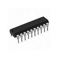
DAC0832LCN National Semiconductor, DAC0832LCN Datasheet - Page 16

DAC0832LCN
Manufacturer Part Number
DAC0832LCN
Description
D/A Converter (D-A) IC
Manufacturer
National Semiconductor
Datasheet
1.DAC0832LCN.pdf
(28 pages)
Specifications of DAC0832LCN
Resolution (bits)
8bit
Data Interface
CMOS, Parallel, TTL
No. Of Pins
20
Settling Time
1µs
Mounting Type
Through Hole
Peak Reflow Compatible (260 C)
No
No. Of Bits
8 Bit
Leaded Process Compatible
No
Number Of Channels
1
Resolution
8b
Interface Type
Parallel
Single Supply Voltage (typ)
Not RequiredV
Dual Supply Voltage (typ)
Not RequiredV
Architecture
R-2R
Power Supply Requirement
Digital
Output Type
Current
Integral Nonlinearity Error
0.2LSB
Single Supply Voltage (min)
Not RequiredV
Single Supply Voltage (max)
Not RequiredV
Dual Supply Voltage (min)
Not RequiredV
Dual Supply Voltage (max)
Not RequiredV
Operating Temp Range
0C to 70C
Operating Temperature Classification
Commercial
Mounting
Through Hole
Pin Count
20
Package Type
PDIP
Lead Free Status / RoHS Status
Contains lead / RoHS non-compliant
Lead Free Status / RoHS Status
Contains lead / RoHS non-compliant
Available stocks
Company
Part Number
Manufacturer
Quantity
Price
Company:
Part Number:
DAC0832LCN
Manufacturer:
NS
Quantity:
6 000
Company:
Part Number:
DAC0832LCN
Manufacturer:
NS
Quantity:
6 000
Part Number:
DAC0832LCN
Manufacturer:
NS/国半
Quantity:
20 000
www.national.com
DAC0830 Series Application Hints
This configuration offers several useful application advan-
tages. Since the output is a voltage, an external op amp is
not necessarily required but the output impedance of the
DAC is fairly high (equal to the specified reference input
resistance of 10 k to 20 k ) so an op amp may be used for
buffering purposes. Some of the advantages of this mode
are illustrated in Figures 12, 13, 14, 15 .
There are two important things to keep in mind when using
this DAC in the voltage switching mode. The applied refer-
ence voltage must be positive since there are internal para-
sitic diodes from ground to the I
which would turn on if the applied reference went negative.
There is also a dependence of conversion linearity and gain
error on the voltage difference between V
applied to the normal current output terminals. This is a
result of the voltage drive requirements of the ladder
switches. To ensure that all 8 switches turn on sufficiently (so
as not to add significant resistance to any leg of the ladder
and thereby introduce additional linearity and gain errors) it
is recommended that the applied reference voltage be kept
less than +5V
V
gain error change. Figures 16, 17, 18 characterize the ef-
fects of bringing V
typical temperature performance of this voltage switching
configuration.
REF
. These restrictions ensure less than 0.1% linearity and
DC
and V
REF
CC
and V
be at least 9V more positive than
CC
closer together as well as
OUT1
and I
FIGURE 10. Adding Full-Scale Adjustment
CC
FIGURE 11. Voltage Mode Switching
and the voltage
OUT2
terminals
(Continued)
16
• Voltage switching mode eliminates output signal inver-
• Zero code output voltage is limited by the low level output
•
sion and therefore a need for a negative power supply.
saturation voltage of the op amp. The 2 k
resistor helps to reduce this voltage.
V
OS
of the op amp has no effect on DAC linearity.
FIGURE 12. Single Supply DAC
00560811
00560812
pull-down
00560841


