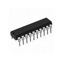
DAC0832LCN National Semiconductor, DAC0832LCN Datasheet - Page 19

DAC0832LCN
Manufacturer Part Number
DAC0832LCN
Description
D/A Converter (D-A) IC
Manufacturer
National Semiconductor
Datasheet
1.DAC0832LCN.pdf
(28 pages)
Specifications of DAC0832LCN
Resolution (bits)
8bit
Data Interface
CMOS, Parallel, TTL
No. Of Pins
20
Settling Time
1µs
Mounting Type
Through Hole
Peak Reflow Compatible (260 C)
No
No. Of Bits
8 Bit
Leaded Process Compatible
No
Number Of Channels
1
Resolution
8b
Interface Type
Parallel
Single Supply Voltage (typ)
Not RequiredV
Dual Supply Voltage (typ)
Not RequiredV
Architecture
R-2R
Power Supply Requirement
Digital
Output Type
Current
Integral Nonlinearity Error
0.2LSB
Single Supply Voltage (min)
Not RequiredV
Single Supply Voltage (max)
Not RequiredV
Dual Supply Voltage (min)
Not RequiredV
Dual Supply Voltage (max)
Not RequiredV
Operating Temp Range
0C to 70C
Operating Temperature Classification
Commercial
Mounting
Through Hole
Pin Count
20
Package Type
PDIP
Lead Free Status / RoHS Status
Contains lead / RoHS non-compliant
Lead Free Status / RoHS Status
Contains lead / RoHS non-compliant
Available stocks
Company
Part Number
Manufacturer
Quantity
Price
Company:
Part Number:
DAC0832LCN
Manufacturer:
NS
Quantity:
6 000
Company:
Part Number:
DAC0832LCN
Manufacturer:
NS
Quantity:
6 000
Part Number:
DAC0832LCN
Manufacturer:
NS/国半
Quantity:
20 000
DAC0830 Series Application Hints
2.8 Miscellaneous Application Hints
These converters are CMOS products and reasonable care
should be exercised in handling them to prevent catastrophic
failures due to static discharge.
Conversion accuracy is only as good as the applied refer-
ence voltage so providing a stable source over time and
temperature changes is an important factor to consider.
A “good” ground is most desirable. A single point ground
distribution technique for analog signals and supply returns
keeps other devices in a system from affecting the output of
the DACs.
(Continued)
Variation vs. Temperature
Gain and Linearity Error
FIGURE 18.
00560834
19
During power-up supply voltage sequencing, the −15V (or
−12V) supply of the op amp may appear first. This will cause
the output of the op amp to bias near the negative supply
potential. No harm is done to the DAC, however, as the
on-chip 15 k feedback resistor sufficiently limits the current
flow from I
diode drop below ground.
Careful circuit construction with minimization of lead lengths
around the analog circuitry, is a primary concern. Good high
frequency supply decoupling will aid in preventing inadvert-
ant noise from appearing on the analog output.
Overall noise reduction and reference stability is of particular
concern when using the higher accuracy versions, the
DAC0830 and DAC0831, or their advantages are wasted.
3.0 GENERAL APPLICATION IDEAS
The connections for the control pins of the digital input
registers are purposely omitted. Any of the control formats
discussed in Section 1 of the accompanying text will work
with any of the circuits shown. The method used depends on
the overall system provisions and requirements.
The digital input code is referred to as D and represents the
decimal equivalent value of the 8-bit binary input, for ex-
ample:
Pin 13
1
1
0
0
0
MSB
1
0
0
0
0
OUT1
1
0
0
0
0
Binary Input
when this lead is internally clamped to one
1
0
1
0
0
1
0
0
0
0
1
0
0
0
0
1
0
0
1
0
Pin 7
LSB
1
0
0
0
0
Equivalent
Decimal
www.national.com
255
128
16
D
2
0


