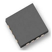
SIP11203DLP-T1-E3 Vishay, SIP11203DLP-T1-E3 Datasheet - Page 8

SIP11203DLP-T1-E3
Manufacturer Part Number
SIP11203DLP-T1-E3
Description
DRIVER, SYNCH RECTIFIER, MLP44-16
Manufacturer
Vishay
Datasheet
1.SIP11203DLP-T1-E3.pdf
(16 pages)
Specifications of SIP11203DLP-T1-E3
Supply Voltage
13V
Digital Ic Case Style
MLP44
No. Of Pins
16
Operating Temperature Range
-40°C To +85°C
Package / Case
MLP44
Base Number
11203
Supply Voltage Max
13V
Supply Voltage Min
5.5V
Svhc
No SVHC (15-Dec-2010)
Rohs Compliant
Yes
Device Type
Power
Lead Free Status / RoHS Status
Lead free / RoHS Compliant
Available stocks
Company
Part Number
Manufacturer
Quantity
Price
Part Number:
SIP11203DLP-T1-E3
Manufacturer:
VISHAY/威世
Quantity:
20 000
SiP11203/SiP11204
Vishay Siliconix
APPLICATIONS INFORMATION
Powering SiP11203/SiP11204
The SiP11203/SiP11204 has an internal pre-regulator
to provide 5 V at V
sub-circuits. This allows the IC to operate from any
input voltage within the allowable V
same time, V
driver outputs (OUTA and OUTB) directly. The gate
drive level to the synchronous rectifier MOSFETs is
determined by V
The V
methods, such as an extra winding on the power trans-
former or on the output inductor. Alternatively, this sup-
Figure 2. Typical schematic showing how the V
START-UP DRIVER OPERATION
During start-up of the SiP11203/SiP11204, the MOS-
FET drivers (OUTA and OUTB) are disabled until V
at 90 % of its final value. To fully prevent any spurious
turn-on of the synchronous rectifier MOSFETs, the
gates of the MOSFETs are held off during this start up
period. Until the main drivers are enabled, the INA and
INB drive paths are re-routed, or “swapped,” inside the
IC. In conjunction with a dedicated n-channel hold-off
MOSFET “inverter” placed in parallel with each main
driver, this allows the IC to ground the appropriate syn-
chronous rectifier gate at the necessary time. See Fig-
ure 3.
If the first two pulses coming through the pulse trans-
former are considered, the following sequence of
events follows:
www.vishay.com
8
IN
voltage can be derived using conventional
IN
provides the supply voltage to the gate
IN
L
, which biases many of the internal
IN
IN
range. At the
SRH
SRL
SRH
SRL
synchronous rectifier timing signals
supply for SiP11203/SiP11204 is generated using the pulse transformer providing the
L
is
ply can be derived from the pulse transformer used to
transmit synchronous rectifier timing signals from the
primary to the secondary, as shown in Figure 2 below.
The voltage level on V
ratio of the pulse transformer and the differential volt-
age between SRL of the Si9122, Si9122A, Si9122E
and SRH of of the Si9122, Si9122A, Si9122E. Note
that this circuit will cause the voltages at INA and INB
to be twice that of V
to limit the voltage seen by INA and INB in order to
avoid exceeding their recommended operating values.
• INA goes low, which would normally command the
• When INA goes low, INB will be driven to a level of
GND
GND
OUTA driver to go low. This would prevent spurious
turn-on of the associated synchronous rectifier.
However, since the voltage to the IC is below its
normal operating level, it cannot be guaranteed that
OUTA can in fact go to its necessary state. For this
reason, the OUTA and OUTB drivers are disabled
while V
2 x V
ary of the pulse transformer is rectified to provide
V
diodes clamping the secondary’s negative excur-
sions one diode drop below ground (See Figure 2).
IN
. Specifically, this results from the rectifier
IN
. This is due to the way in which the second-
L
INA
V
INB
INA
V
INB
< UVLO
IN
IN
SiP11203
SiP11204
SiP11203
SiP11203
SiP11204
SiP11204
IN
R
.
. Therefore it may be necessary
IN
will be determined by the turn
S-61082–Rev. B, 19-Jun-06
Document Number: 73868


