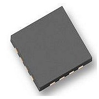
SIP11203DLP-T1-E3 Vishay, SIP11203DLP-T1-E3 Datasheet - Page 2

SIP11203DLP-T1-E3
Manufacturer Part Number
SIP11203DLP-T1-E3
Description
DRIVER, SYNCH RECTIFIER, MLP44-16
Manufacturer
Vishay
Datasheet
1.SIP11203DLP-T1-E3.pdf
(16 pages)
Specifications of SIP11203DLP-T1-E3
Supply Voltage
13V
Digital Ic Case Style
MLP44
No. Of Pins
16
Operating Temperature Range
-40°C To +85°C
Package / Case
MLP44
Base Number
11203
Supply Voltage Max
13V
Supply Voltage Min
5.5V
Svhc
No SVHC (15-Dec-2010)
Rohs Compliant
Yes
Device Type
Power
Lead Free Status / RoHS Status
Lead free / RoHS Compliant
Available stocks
Company
Part Number
Manufacturer
Quantity
Price
Part Number:
SIP11203DLP-T1-E3
Manufacturer:
VISHAY/威世
Quantity:
20 000
SiP11203/SiP11204
Vishay Siliconix
Notes:
a. Device mounted with all leads soldered to printed circuit board.
Stresses beyond those listed under “Absolute Maximum Ratings” may cause permanent damage to the device. These are stress ratings only, and functional operation
of the device at these or any other conditions beyond those indicated in the operational sections of the specifications is not implied. Exposure to absolute maximum
rating conditions for extended periods may affect device reliability.
www.vishay.com
2
ABSOLUTE MAXIMUM RATINGS
Parameter
V
V
Storage Temperature
Junction Temperature
Package Thermal Impedance (Rθ
RECOMMENDED OPERATING RANGE
Parameter
V
C
C
C
Linear Inputs (EA+, EA-, OVP
Error Amplifier Output Voltage
Logic Inputs (IN
Reference voltage output current
R
C
SPECIFICATIONS
Parameter
Power Supply
V
V
V
V
V
Supply Current
Quiescent Current
Start-up Current Capability
Reference Voltages
V
V
V
V
Internal Buffered Reference Voltage
IN
REF
IN
L
L
L
L
L
REF
REF
REF
REF
VIN
VL
REF
PD
PD
Output Voltage
Temperature Coefficient
Line Regulation
Load Regulation
Supply PSRR
, IN
, Linear Inputs
Voltage
Temperature Coefficient
Load Regulation
PSRR
A
, IN
B
A
, IN
B
)
IN
)
JA
)
V
V
I
V
Symbol
REF_PSRR
V
STARTUP
V
V
REF_LDR
L_PSRR
V
REFINT
TC1
L_LNR
L_LDR
TC2
V
I
I
REF
IN
Q
L
16 Pin 44MLP
Package Power Dissipation (package)
V
V
IN
IN
= 5.5 V, C
= 7.5 V, C
Current sourced from V
Device switching disabled (Note e)
I
V
L
Unless Otherwise Specified
IN
V
= 0 mA to 3.3 mA, V
IN
I
Output disabled (Note e)
= 5.5 V, measured at R
f
f
REF2
TEST
LOAD(A)
LOAD(A)
TEST
= 5.5 V, I
5.5 V ≤ V
T
Test Conditions
A
= 0 mA, T
I
= 100 Hz, (Note c)
= - 40 to 85 °C
=100 Hz, (Note c)
REF2
I
(Note c)
L
(Note c)
= C
= C
= 0 mA
REF
= 0 mA
LOAD(B)
LOAD(B)
IN
= 0 to 10 µA
≤ 13 V
IN
A
= 25 °C
to V
IN
= 6 nF (Note c, d)
= 6 nF (Note c, d)
= 5.5 V
a
L
PD
, V
pin
L
= 0 V
- 0.3 V to V
- 65 to + 160
- 40 to +125
5.5 to 13
0 to 3.5
1.212
1.188
2.320
0 to V
0 to 13
1 to 10
Min
4.75
Limit
Limit
> 15
35
0.1
15
745
10
47
1
1
a
L
L
+ 0.3 V
S-61082–Rev. B, 19-Jun-06
Limits
Document Number: 73868
1.225
1.225
Typ
15.5
160
160
5.0
1.2
3.5
1.5
2.5
70
12
45
60
3
b
1.238
1.262
2.570
Max
5.25
4.5
2.5
10
55
8
a
°C/W
Unit
Unit
mW
µA
kΩ
°C
µF
V
V
V
nF
µV/°C
µV/°C
Unit
mV
mA
mV
dB
dB
V
V
V


