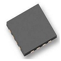
SIP11203DLP-T1-E3 Vishay, SIP11203DLP-T1-E3 Datasheet - Page 13

SIP11203DLP-T1-E3
Manufacturer Part Number
SIP11203DLP-T1-E3
Description
DRIVER, SYNCH RECTIFIER, MLP44-16
Manufacturer
Vishay
Datasheet
1.SIP11203DLP-T1-E3.pdf
(16 pages)
Specifications of SIP11203DLP-T1-E3
Supply Voltage
13V
Digital Ic Case Style
MLP44
No. Of Pins
16
Operating Temperature Range
-40°C To +85°C
Package / Case
MLP44
Base Number
11203
Supply Voltage Max
13V
Supply Voltage Min
5.5V
Svhc
No SVHC (15-Dec-2010)
Rohs Compliant
Yes
Device Type
Power
Lead Free Status / RoHS Status
Lead free / RoHS Compliant
Available stocks
Company
Part Number
Manufacturer
Quantity
Price
Part Number:
SIP11203DLP-T1-E3
Manufacturer:
VISHAY/威世
Quantity:
20 000
OUTPUT OVER-VOLTAGE PROTECTION
The SiP11203/SiP11204 provide output over-voltage
protection (OVP) by means of a dedicated internal
comparator. One input of the OVP comparator is
brought out to the OVP
to an internal reference voltage that is fixed at 120 %
of the 1.225 V V
cess of 1.47 V at the OVP
The OVP circuitry operates in two different ways, de-
pending upon whether the SiP11203/SiP11204 is in
start-up mode, or in normal operation. In this context,
start-up mode is defined as device operation during
that period for which V
value, or 1.1 V.
Start-Up Mode:
If the 1.47 V OVP threshold is exceeded during start-
up, the driver outputs OUTA and OUTB are held low
until the voltage on the V
The driver outputs are then released to respond to INA
and INB.
Normal Operation Mode:
If the OVP threshold is exceeded, or remains exceed-
ed, after V
set. This will cause the driver outputs to be forced high
Document Number: 73868
S-61082–Rev. B, 19-Jun-06
Figure 8. The delay of SiP11203 and SiP11204 gate-drive output signals compensate the break-before-make switching action
REF
has reached 1.1 V, the OVP latch will be
REF
value, or 1.47 V. A voltage in ex-
REF
IN
is less than 90 % of its 1.225 V
pin, and the other is returned
REF
IN
pin indicates an OVP fault.
pin has exceeded 1.1 V.
BBM1
PWM
OUT A
discrepancies arising from propagation delays
DL
BBM2
PWM
delay set by R
Rising edge
BBM3
for SiP11203, or forced low for SiP11204. At the same
time, an on-chip transistor will discharge the bypass
capacitor at the V
latch is reset when the logical and of two conditions:
When the OVP latch is reset, the SiP11203/SiP11204
will release their outputs, and return to normal opera-
tion via a soft-start cycle.
To prevent spurious activation of the over-voltage func-
tion, the over-voltage condition must be present for five
switching instances, where a switching instance is de-
fined as activity on either IN
ing instance the overvoltage condition is latched. If the
over voltage condition disappears the IC will not recog-
nize an over-voltage as being present and the counter
will be reset to zero.
Note that the OVP
the internal 2.5 V reference voltage V
derived from V
rise time of either V
PWM
• The voltage on the V
• The voltage at the OVP
OUT A
DL
of its nominal 1.225 V level, to ensure an orderly
soft-start cycle when operation resumes, and
cating that the OVP fault has been cleared.
DEL
BBM4
PWM
IN
, and therefore is not delayed by the
REF
IN
L
threshold voltage is derived from
SiP11203/SiP11204
or V
REF
pin towards ground. The OVP
REF
pin must be ≤ 20 % (245 mV)
A
IN
.
or IN
pin must be 1.1 V, indi-
Vishay Siliconix
B
. On the fifth switch-
REFINT
www.vishay.com
, which is
13


