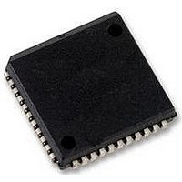
SC28L92A1A NXP Semiconductors, SC28L92A1A Datasheet - Page 48

SC28L92A1A
Manufacturer Part Number
SC28L92A1A
Description
UART, DUAL, 3.3V OR 5V, SMD, 28L92
Manufacturer
NXP Semiconductors
Datasheet
1.SC28L92A1B557.pdf
(73 pages)
Specifications of SC28L92A1A
No. Of Channels
2
Supply Voltage Range
2.97V To 3.63V, 4.5V To 5.5V
Operating Temperature Range
-40°C To +85°C
Digital Ic Case Style
PLCC
No. Of Pins
44
Svhc
No SVHC (18-Jun-2010)
Operating
RoHS Compliant
Data Rate
230.4Kilobaud
Uart Features
Programmable Channel Mode, Line Break Detection & Generation
Rohs Compliant
Yes
Available stocks
Company
Part Number
Manufacturer
Quantity
Price
Company:
Part Number:
SC28L92A1A
Manufacturer:
NXP
Quantity:
677
Company:
Part Number:
SC28L92A1A,512
Manufacturer:
NXP Semiconductors
Quantity:
10 000
Company:
Part Number:
SC28L92A1A,518
Manufacturer:
NXP Semiconductors
Quantity:
10 000
Company:
Part Number:
SC28L92A1A,529
Manufacturer:
NXP Semiconductors
Quantity:
10 000
Company:
Part Number:
SC28L92A1A529
Manufacturer:
NXP Semiconductors
Quantity:
135
NXP Semiconductors
SC28L92_7
Product data sheet
7.3.13 Interrupt Vector Register (IVR; 68xxx mode) or General Purpose register
7.3.14 Counter/timer registers
(GP; 80xxx mode)
This register stores the Interrupt Vector. It is initialized to 0x0F on hardware reset and is
usually changed from this value during initialization of the SC28L92. The contents of this
register will be placed on the data bus when IACKN is asserted LOW or a read of address
0xC is performed.
When not operating in the 68xxx mode, this register may be used as a general purpose
one byte storage register. A convenient use could be to store a shadow of the contents of
another SC28L92 register (IMR, for example).
Table 61.
Table 62.
Table 63.
The CTPU and CTPL hold the eight MSBs and eight LSBs, respectively, of the value to be
used by the counter/timer in either the counter or timer modes of operation. The minimum
value which may be loaded into the CTPU/CTPL registers is 0x0002. Note that these
registers are write only and cannot be read by the CPU.
In the timer mode, the C/T generates a square wave whose period is twice the value (in
C/T clock periods) of the CTPU and CTPL. The waveform so generated is often used for a
data clock. The formula for calculating the divisor n to load to the CTPU and CTPL for a
particular 1 data clock is shown in
n
Often this division will result in a non-integer number; 26.3, for example. One can only
program integer numbers in a digital divider. Therefore, 26 would be chosen. This gives a
baud rate error of 0.3/26.3 which is 1.14 %; well within the ability asynchronous mode of
operation.
The C/T will not be running until it receives an initial start counter command (read at
address A3 to A0 = 1110). After this, while in timer mode, the C/T will run continuously.
Receipt of a start counter command (read with A3 to A0 = 1110) causes the counter to
terminate the current timing cycle and to begin a new cycle using the values in CTPU and
CTPL. If the value in CTPU and CTPL is changed, the current half-period will not be
affected, but subsequent half periods will be affected.
Bit
7:0
Bit
7:0
=
counter/timer clock frequency
---------------------------------------------------------------------------------- -
7
2 16
Symbol
-
Symbol
-
IVR/GP - Interrupt vector register or general purpose register (address 0xC)
bit allocation
CTPU - Counter/Timer Preset Upper register (address 0x6) bit description
CTPL - Counter/Timer preset Lower register (address 0x7) bit description
desired baud rate
interrupt vector (68xxx mode) or one byte storage (80xxx mode)
6
Description
The upper eight (8) bits for the 16-bit counter/timer preset register
Description
The lower eight (8) bits for the 16-bit counter/timer preset register
Rev. 07 — 19 December 2007
3.3 V/5.0 V Dual Universal Asynchronous Receiver/Transmitter
5
Equation
4
2.
3
2
SC28L92
© NXP B.V. 2007. All rights reserved.
1
48 of 73
0
(2)


