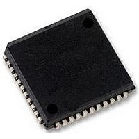
SC28L92A1A NXP Semiconductors, SC28L92A1A Datasheet - Page 37

SC28L92A1A
Manufacturer Part Number
SC28L92A1A
Description
UART, DUAL, 3.3V OR 5V, SMD, 28L92
Manufacturer
NXP Semiconductors
Datasheet
1.SC28L92A1B557.pdf
(73 pages)
Specifications of SC28L92A1A
No. Of Channels
2
Supply Voltage Range
2.97V To 3.63V, 4.5V To 5.5V
Operating Temperature Range
-40°C To +85°C
Digital Ic Case Style
PLCC
No. Of Pins
44
Svhc
No SVHC (18-Jun-2010)
Operating
RoHS Compliant
Data Rate
230.4Kilobaud
Uart Features
Programmable Channel Mode, Line Break Detection & Generation
Rohs Compliant
Yes
Available stocks
Company
Part Number
Manufacturer
Quantity
Price
Company:
Part Number:
SC28L92A1A
Manufacturer:
NXP
Quantity:
677
Company:
Part Number:
SC28L92A1A,512
Manufacturer:
NXP Semiconductors
Quantity:
10 000
Company:
Part Number:
SC28L92A1A,518
Manufacturer:
NXP Semiconductors
Quantity:
10 000
Company:
Part Number:
SC28L92A1A,529
Manufacturer:
NXP Semiconductors
Quantity:
10 000
Company:
Part Number:
SC28L92A1A529
Manufacturer:
NXP Semiconductors
Quantity:
135
NXP Semiconductors
SC28L92_7
Product data sheet
7.3.4.1 Status Register channel A (SRA)
7.3.4 Status registers
Table 41.
[1]
Table 42.
Bit
7
6
5
received
break
These status bits are appended to the corresponding data character in the receive FIFO. A read of the
status provides these bits [7:5] from the top of the FIFO together with bits [4:0]. These bits are cleared by a
reset error status command. In character mode they are discarded when the corresponding data character
is read from the FIFO. In block error mode, the error-reset command (command 0x4 or receiver reset) must
used to clear block error conditions.
7
Symbol
-
-
-
[1]
SRA - Status register channel A (address 0x1) bit allocation
SRA - Status register channel A (address 0x1) bit description
framing
error
6
Description
Channel A received break.
This bit indicates that an all zero character of the programmed length has been
received without a stop bit. Only a single FIFO position is occupied when a
break is received: further entries to the FIFO are inhibited until the RxDA line
returns to the marking state for at least one-half a bit time two successive
edges of the internal or external 1 clock. This will usually require a HIGH
time of one X1 clock period or 3 X1 edges since the clock of the controller
is not synchronous to the X1 clock.
When this bit is set, the channel A change in break bit in the ISR (ISR[2]) is set.
ISR[2] is also set when the end of the break condition, as defined above, is
detected.
The break detect circuitry can detect breaks that originate in the middle of a
received character. However, if a break begins in the middle of a character, it
must persist until at least the end of the next character time in order for it to be
detected.
This bit is reset by command 0x4 (0100) written to the command register or by
receiver reset.
Channel A framing error.
This bit, when set, indicates that a stop bit was not detected (not a logic 1)
when the corresponding data character in the FIFO was received. The stop bit
check is made in the middle of the first stop bit position.
Channel A parity error.
This bit is set when the with parity or force parity mode is programmed and the
corresponding character in the FIFO was received with incorrect parity.
In the special multi-drop mode the parity error bit stores the receive A/D
(Address/Data) bit.
[1]
0 = no
1 = yes
0 = no
1 = yes
0 = no
1 = yes
Rev. 07 — 19 December 2007
3.3 V/5.0 V Dual Universal Asynchronous Receiver/Transmitter
error
parity
5
[1]
overrun
error
4
TxEMTA
3
TxRDYA
2
RxFULLA
SC28L92
© NXP B.V. 2007. All rights reserved.
1
RxRDYA
37 of 73
0


