FB180SA10P Vishay, FB180SA10P Datasheet - Page 3
FB180SA10P
Manufacturer Part Number
FB180SA10P
Description
MOSFET Power N-Chan 100V 180 Amp
Manufacturer
Vishay
Datasheet
1.FB180SA10P.pdf
(8 pages)
Specifications of FB180SA10P
Transistor Polarity
N-Channel
Minimum Operating Temperature
- 55 C
Configuration
Single Dual Source
Resistance Drain-source Rds (on)
0.0065 Ohm @ 10 V
Drain-source Breakdown Voltage
100 V
Gate-source Breakdown Voltage
+/- 20 V
Continuous Drain Current
180 A
Power Dissipation
480000 mW
Maximum Operating Temperature
+ 150 C
Mounting Style
SMD/SMT
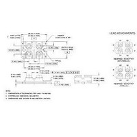
Package / Case
SOT-227
Continuous Drain Current Id
180A
Drain Source Voltage Vds
100V
On Resistance Rds(on)
6.5mohm
Rds(on) Test Voltage Vgs
10V
Threshold Voltage Vgs Typ
4V
Lead Free Status / RoHS Status
Lead free / RoHS Compliant
Lead Free Status / RoHS Status
Lead free / RoHS Compliant, Lead free / RoHS Compliant
Available stocks
Company
Part Number
Manufacturer
Quantity
Price
Company:

Part Number:
FB180SA10P
Manufacturer:
VISHAY
Quantity:
340
Part Number:
FB180SA10P
Manufacturer:
VISHAY/威世
Quantity:
20 000


Document Number: 94541
Revision: 30-Jul-10
1000
1000
1000
100
100
100
10
10
10
1
1
1
0.1
0.1
4
TOP
BOTTOM
Fig. 3 - Typical Transfer Characteristics
TOP
BOTTOM
Fig. 1 - Typical Output Characteristics
Fig. 2 - Typical Output Characteristics
T = 150 C
V
V
J
V
DS
DS
5
VGS
15V
10V
8.0V
7.0V
6.0V
5.5V
5.0V
4.5V
VGS
15V
10V
8.0V
7.0V
6.0V
5.5V
5.0V
4.5V
GS
, Drain-to-Source Voltage (V)
, Drain-to-Source Voltage (V)
T = 25 C
, Gate-to-Source Voltage (V)
J
°
6
1
1
°
DiodesAmericas@vishay.com, DiodesAsia@vishay.com,
4.5V
For technical questions within your region, please contact one of the following:
7
4.5V
20µs PULSE WIDTH
T = 25 C
20μs PULSE WIDTH
T = 150 C
V
20µs PULSE WIDTH
J
J
DS
10
10
8
= 25V
°
°
9
100
100
10
Power MOSFET, 180 A
Fig. 4 - Normalized On-Resistance vs. Temperature
20000
15000
10000
5000
DiodesEurope@vishay.com
2.5
2.0
1.5
1.0
0.5
0.0
20
15
10
0
5
0
-60 -40 -20
0
1
I =
I =
D
D
Fig. 6 - Typical Gate Charge vs.
Fig. 5 - Typical Capacitance vs.
180A
50
180 A
V
T , Junction Temperature( C)
DS
Drain to Source Voltage
Q , Total Gate Charge (nC)
J
Gate to Source Voltage
C
C
C
100
G
V
C
C
C
oss
iss
rss
, Drain-to-Source Voltage (V)
0
GS
iss
rss
oss
Vishay Semiconductors
20
=
=
=
=
150
0V,
C
C
C
gs
gd
ds
40
200
+ C
+ C
10
V
V
V
60
f = 1MHz
gd ,
gd
DS
DS
DS
FOR TEST CIRCUIT
SEE FIGURE
250
80 100 120 140 160
= 80V
= 50V
= 20V
FB180SA10P
C
ds
300
V
SHORTED
°
GS
350
=
10V
13
www.vishay.com
400
100
3
Related parts for FB180SA10P
Image
Part Number
Description
Manufacturer
Datasheet
Request
R


Part Number:
Description:
357-036-542-201 CARDEDGE 36POS DL .156 BLK LOPRO
Manufacturer:
Vishay
Datasheet:
Part Number:
Description:
357-036-542-201 CARDEDGE 36POS DL .156 BLK LOPRO
Manufacturer:
Vishay
Datasheet:
Part Number:
Description:
357-036-542-201 CARDEDGE 36POS DL .156 BLK LOPRO
Manufacturer:
Vishay
Datasheet:
Part Number:
Description:
357-036-542-201 CARDEDGE 36POS DL .156 BLK LOPRO
Manufacturer:
Vishay
Datasheet:
Part Number:
Description:
357-036-542-201 CARDEDGE 36POS DL .156 BLK LOPRO
Manufacturer:
Vishay
Datasheet:
Part Number:
Description:
357-036-542-201 CARDEDGE 36POS DL .156 BLK LOPRO
Manufacturer:
Vishay
Datasheet:
Part Number:
Description:
357-036-542-201 CARDEDGE 36POS DL .156 BLK LOPRO
Manufacturer:
Vishay
Datasheet:
Part Number:
Description:
357-036-542-201 CARDEDGE 36POS DL .156 BLK LOPRO
Manufacturer:
Vishay
Datasheet:
Part Number:
Description:
357-036-542-201 CARDEDGE 36POS DL .156 BLK LOPRO
Manufacturer:
Vishay
Datasheet:
Part Number:
Description:
357-036-542-201 CARDEDGE 36POS DL .156 BLK LOPRO
Manufacturer:
Vishay
Datasheet:
Part Number:
Description:
357-036-542-201 CARDEDGE 36POS DL .156 BLK LOPRO
Manufacturer:
Vishay
Datasheet:
Part Number:
Description:
357-036-542-201 CARDEDGE 36POS DL .156 BLK LOPRO
Manufacturer:
Vishay
Datasheet:
Part Number:
Description:
357-036-542-201 CARDEDGE 36POS DL .156 BLK LOPRO
Manufacturer:
Vishay
Datasheet:
Part Number:
Description:
357-036-542-201 CARDEDGE 36POS DL .156 BLK LOPRO
Manufacturer:
Vishay
Datasheet: