FB180SA10P Vishay, FB180SA10P Datasheet - Page 2
FB180SA10P
Manufacturer Part Number
FB180SA10P
Description
MOSFET Power N-Chan 100V 180 Amp
Manufacturer
Vishay
Datasheet
1.FB180SA10P.pdf
(8 pages)
Specifications of FB180SA10P
Transistor Polarity
N-Channel
Minimum Operating Temperature
- 55 C
Configuration
Single Dual Source
Resistance Drain-source Rds (on)
0.0065 Ohm @ 10 V
Drain-source Breakdown Voltage
100 V
Gate-source Breakdown Voltage
+/- 20 V
Continuous Drain Current
180 A
Power Dissipation
480000 mW
Maximum Operating Temperature
+ 150 C
Mounting Style
SMD/SMT
Package / Case
SOT-227
Continuous Drain Current Id
180A
Drain Source Voltage Vds
100V
On Resistance Rds(on)
6.5mohm
Rds(on) Test Voltage Vgs
10V
Threshold Voltage Vgs Typ
4V
Lead Free Status / RoHS Status
Lead free / RoHS Compliant
Lead Free Status / RoHS Status
Lead free / RoHS Compliant, Lead free / RoHS Compliant
Available stocks
Company
Part Number
Manufacturer
Quantity
Price
Company:

Part Number:
FB180SA10P
Manufacturer:
VISHAY
Quantity:
340
Part Number:
FB180SA10P
Manufacturer:
VISHAY/威世
Quantity:
20 000


FB180SA10P
Vishay Semiconductors
Note
(1)
Notes
(1)
(2)
www.vishay.com
2
THERMAL RESISTANCE
PARAMETER
Junction to case
Case to sink, flat, greased surface
ELECTRICAL CHARACTERISTICS (T
PARAMETER
Drain to source breakdown voltage
Breakdown voltage temperature
coefficient
Static drain to source on-resistance
Gate threshold voltage
Forward transconductance
Drain to source leakage current
Gate to source forward leakage
Total gate charge
Gate to source charge
Gate to drain ("Miller") charge
Turn-on delay time
Rise time
Turn-off delay time
Fall time
Internal source inductance
Input capacitance
Output capacitance
Reverse transfer capacitance
SOURCE-DRAIN RATINGS AND CHARACTERISTICS
PARAMETER
Continuous source current
(body diode)
Pulsed source current (body diode)
Diode forward voltage
Reverse recovery time
Reverse recovery charge
Forward turn-on time
Pulse width 300 μs, duty cycle 2 %
Repetitive rating; pulse width limited by maximum junction temperature (see fig. 8)
Pulse width 300 μs, duty cycle 2 %
DiodesAmericas@vishay.com, DiodesAsia@vishay.com,
For technical questions within your region, please contact one of the following:
V
SYMBOL
SYMBOL
R
SYMBOL
V(
(BR)DSS
DS(on)
V
V
I
SM
R
R
t
t
C
t
BR)DSS
I
I
Q
C
C
GS(th)
Q
SD
d(on)
d(off)
rr
Q
g
DSS
GSS
Q
t
L
I
thJC
thCS
t
on
t
oss
rss
S
gd
iss
fs
gs
r
f
S
(2)
rr
g
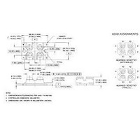
Power MOSFET, 180 A
J
(1)
(2)
= 25 °C unless otherwise noted)
/T
(1)
J
MOSFET symbol
showing the integral
reverse p-n junction diode.
T
T
Intrinsic turn-on time is negligible (turn-on is dominated by L
V
Reference to 25 °C, I
V
V
V
V
V
V
V
I
V
V
V
I
R
R
Between lead, and center of die contact
V
V
f = 1.0 MHz, see fig. 5
D
D
J
J
GS
GS
DS
DS
DS
DS
GS
GS
DS
GS
DD
GS
DS
g
D
= 180 A
= 180 A
= 25 °C, I
= 25 °C, I
= 2.0(internal)
= 0.27, see fig. 10
= 0 V, I
= 10 V, I
= V
= 25 V, I
= 100 V, V
= 80 V, V
= 20 V
= - 20 V
= 80 V
= 10.0 V; see fig. 6 and 13
= 50 V
= 0 V
= 25 V
GS
TEST CONDITIONS
TEST CONDITIONS
, I
TYP.
0.05
D
D
S
D
D
F
-
= 250 μA
GS
= 250 μA
= 180 A, V
= 180 A
= 180 A; dI/dt = 100 A/μs
= 180 A
GS
= 0 V, T
= 0 V
D
DiodesEurope@vishay.com
= 1 mA
J
(1)
GS
= 125 °C
= 0 V
G
(1)
D
S
MAX.
0.26
-
MIN.
MIN.
100
2.0
93
-
-
-
-
-
-
-
-
-
-
-
-
-
-
-
-
-
-
-
-
-
-
0.0065
10 700
0.093
TYP.
2800
1300
Document Number: 94541
TYP.
250
110
351
181
335
300
5.0
2.6
40
45
-
-
-
-
-
-
-
-
-
-
Revision: 30-Jul-10
S
MAX.
MAX.
- 200
+ L
500
200
380
165
180
720
450
4.0
1.3
3.9
50
60
UNITS
-
-
-
-
-
-
-
-
-
-
-
-
°C/W
D
)
UNITS
UNITS
V/°C
μA
nA
nC
nH
μC
ns
pF
ns
V
V
S
A
V
Related parts for FB180SA10P
Image
Part Number
Description
Manufacturer
Datasheet
Request
R


Part Number:
Description:
357-036-542-201 CARDEDGE 36POS DL .156 BLK LOPRO
Manufacturer:
Vishay
Datasheet:
Part Number:
Description:
357-036-542-201 CARDEDGE 36POS DL .156 BLK LOPRO
Manufacturer:
Vishay
Datasheet:
Part Number:
Description:
357-036-542-201 CARDEDGE 36POS DL .156 BLK LOPRO
Manufacturer:
Vishay
Datasheet:
Part Number:
Description:
357-036-542-201 CARDEDGE 36POS DL .156 BLK LOPRO
Manufacturer:
Vishay
Datasheet:
Part Number:
Description:
357-036-542-201 CARDEDGE 36POS DL .156 BLK LOPRO
Manufacturer:
Vishay
Datasheet:
Part Number:
Description:
357-036-542-201 CARDEDGE 36POS DL .156 BLK LOPRO
Manufacturer:
Vishay
Datasheet:
Part Number:
Description:
357-036-542-201 CARDEDGE 36POS DL .156 BLK LOPRO
Manufacturer:
Vishay
Datasheet:
Part Number:
Description:
357-036-542-201 CARDEDGE 36POS DL .156 BLK LOPRO
Manufacturer:
Vishay
Datasheet:
Part Number:
Description:
357-036-542-201 CARDEDGE 36POS DL .156 BLK LOPRO
Manufacturer:
Vishay
Datasheet:
Part Number:
Description:
357-036-542-201 CARDEDGE 36POS DL .156 BLK LOPRO
Manufacturer:
Vishay
Datasheet:
Part Number:
Description:
357-036-542-201 CARDEDGE 36POS DL .156 BLK LOPRO
Manufacturer:
Vishay
Datasheet:
Part Number:
Description:
357-036-542-201 CARDEDGE 36POS DL .156 BLK LOPRO
Manufacturer:
Vishay
Datasheet:
Part Number:
Description:
357-036-542-201 CARDEDGE 36POS DL .156 BLK LOPRO
Manufacturer:
Vishay
Datasheet:
Part Number:
Description:
357-036-542-201 CARDEDGE 36POS DL .156 BLK LOPRO
Manufacturer:
Vishay
Datasheet: