ZXMN6A25GTA Diodes Inc, ZXMN6A25GTA Datasheet
ZXMN6A25GTA
Specifications of ZXMN6A25GTA


Related parts for ZXMN6A25GTA


ZXMN6A25GTA Summary of contents
Page 1
... Low gate drive • SOT223 package Applications • DC-DC converters • Power management functions • Disconnect switches • Motor control Ordering information Device Reel size (inches) ZXMN6A25GTA 7 Device marking ZXMN 6A25 Issue 2 - November 2006 © Zetex Semiconductors plc 2006 ( ) I ( 10V 6 4.5V 5.7 ...
Page 2
Absolute maximum ratings Parameter Drain-source voltage Gate-source voltage Continuous drain current (c) Pulsed drain current Continuous source current (body diode) Pulsed source current (body diode) Power dissipation 25°C amb Linear derating factor Power dissipation ...
Page 3
Typical characteristics Issue 2 - November 2006 © Zetex Semiconductors plc 2006 ZXMN6A25G 3 www.zetex.com ...
Page 4
Electrical characteristics (at T Parameter STATIC Drain-source breakdown voltage Zero gate voltage drain current Gate-body leakage Gate-source threshold voltage Static drain-source on-state (*) resistance (*) (‡) Forward transconductance (‡) Dynamic Input capacitance Output capacitance Reverse transfer capacitance (†) (‡) Switching ...
Page 5
Typical characteristics Issue 2 - November 2006 © Zetex Semiconductors plc 2006 ZXMN6A25G 5 www.zetex.com ...
Page 6
Typical characteristics Charge Basic gate charge waveform V DS 90% 10 d(on (on) Switching time waveforms Issue 2 - November 2006 © Zetex Semiconductors plc 2006 ...
Page 7
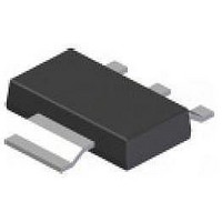
Package outline - SOT223 DIM Millimeters Min Max A - 1.80 A1 0.02 0.10 b 0.66 0.84 b2 2.90 3.10 C 0.23 0.33 D 6.30 6.70 Note: Controlling dimensions are in millimeters. Approximate dimensions are provided in inches. Issue 2 ...
Page 8
Definitions Product change Zetex Semiconductors reserves the right to alter, without notice, specifications, design, price or conditions of supply of any product or service. Customers are solely responsible for obtaining the latest relevant information before placing orders. Applications disclaimer The ...