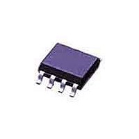
HV9910BLG-G Supertex, HV9910BLG-G Datasheet - Page 6

HV9910BLG-G
Manufacturer Part Number
HV9910BLG-G
Description
LED Drivers UNIVRSL HI BRGHTNES LED DRIVER
Manufacturer
Supertex
Datasheet
1.HV9910BNG-G.pdf
(8 pages)
Specifications of HV9910BLG-G
Low Level Output Current
165000 uA (Min)
High Level Output Current
165000 uA (Min)
Operating Supply Voltage
8 V to 450 V
Maximum Power Dissipation
630 mW
Maximum Operating Temperature
+ 150 C
Mounting Style
SMD/SMT
Package / Case
SOIC-8 Narrow
Minimum Operating Temperature
- 40 C
Operating Supply Voltage (typ)
9/12/15/18/24V
Operating Temperature (min)
-40C
Operating Temperature (max)
150C
Operating Temperature Classification
Automotive
Package Type
SOIC N
Pin Count
8
Mounting
Surface Mount
Lead Free Status / RoHS Status
Lead free / RoHS Compliant
Available stocks
Company
Part Number
Manufacturer
Quantity
Price
Company:
Part Number:
HV9910BLG-G
Manufacturer:
ST
Quantity:
1 000
Part Number:
HV9910BLG-G
Manufacturer:
SUPERTE
Quantity:
20 000
Block Diagram
Pin Description
8-Lead SOIC
1
2
3
4
5
6
7
8
-
Supertex inc.
Pin #
16-Lead SOIC
2, 3, 6, 7, 10,
11, 15, 16
VIN
CS
LD
12
13
14
1
4
5
8
9
250mV
GND
●
Function Description
Regulator
PWMD
1235 Bordeaux Drive, Sunnyvale, CA 94089
GATE
GND
VDD
VIN
CS
NC
LD
RT
+
+
-
-
RT
This pin is the input of an 8.0 - 450V linear regulator.
This pin is the current sense pin used to sense the FET current by means
of an external sense resistor. When this pin exceeds the lower of either the
internal 250mV or the voltage at the LD pin, the GATE output goes low.
Ground return for all internal circuitry. This pin must be electrically con-
nected to the ground of the power train.
This pin is the output GATE driver for an external N-channel power
MOSFET.
This is the PWM dimming input of the IC. When this pin is pulled to GND,
the GATE driver is turned off. When the pin is pulled high, the GATE driver
operates normally.
This is the power supply pin for all internal circuits.
It must be bypassed with a low ESR capacitor to GND (≥0.1μF).
This pin is the linear dimming input and sets the current sense threshold as
long as the voltage at the pin is less than 250mV (typ).
This pin sets the oscillator frequency. When a resistor is connected be-
tween RT and GND, the HV9910B operates in constant frequency mode.
When the resistor is connected between RT and GATE, the IC operates in
constant off-time mode.
No connection
Oscillator
Blanking
6
POR
R Q
S
PWMD
●
Tel: 408-222-8888
●
VDD
GATE
www.supertex.com
HV9910B


