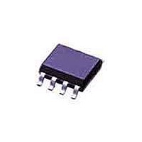
HV9910BLG-G Supertex, HV9910BLG-G Datasheet - Page 5

HV9910BLG-G
Manufacturer Part Number
HV9910BLG-G
Description
LED Drivers UNIVRSL HI BRGHTNES LED DRIVER
Manufacturer
Supertex
Datasheet
1.HV9910BNG-G.pdf
(8 pages)
Specifications of HV9910BLG-G
Low Level Output Current
165000 uA (Min)
High Level Output Current
165000 uA (Min)
Operating Supply Voltage
8 V to 450 V
Maximum Power Dissipation
630 mW
Maximum Operating Temperature
+ 150 C
Mounting Style
SMD/SMT
Package / Case
SOIC-8 Narrow
Minimum Operating Temperature
- 40 C
Operating Supply Voltage (typ)
9/12/15/18/24V
Operating Temperature (min)
-40C
Operating Temperature (max)
150C
Operating Temperature Classification
Automotive
Package Type
SOIC N
Pin Count
8
Mounting
Surface Mount
Lead Free Status / RoHS Status
Lead free / RoHS Compliant
Available stocks
Company
Part Number
Manufacturer
Quantity
Price
Company:
Part Number:
HV9910BLG-G
Manufacturer:
ST
Quantity:
1 000
Part Number:
HV9910BLG-G
Manufacturer:
SUPERTE
Quantity:
20 000
Current Sense
The current sense input of the HV9910B goes to the non-
inverting inputs of two comparators. The inverting terminal
of one comparator is tied to an internal 250mV reference
whereas the inverting terminal of the other comparator is
connected to the LD pin. The outputs of both these com-
parators are fed into an OR GATE and the output of the OR
GATE is fed into the reset pin of the flip-flop. Thus, the com-
parator which has the lowest voltage at the inverting terminal
determines when the GATE output is turned off.
The outputs of the comparators also include a 150-280ns
blanking time which prevents spurious turn-offs of the exter-
nal FET due to the turn-on spike normally present in peak
current mode control. In rare cases, this internal blanking
might not be enough to filter out the turn-on spike. In these
cases, an external RC filter needs to be added between the
external sense resistor (R
Please note that the comparators are fast (with a typical
80ns response time). Hence these comparators are more
susceptible to be triggered by noise than the comparators
of the HV9910. A proper layout minimizing external induc-
tances will prevent false triggering of these comparators.
Oscillator
The oscillator in the HV9910B is controlled by a single re-
sistor connected at the RT pin. The equation governing the
oscillator time period t
If the resistor is connected between RT and GND, HV9910B
operates in a constant frequency mode and the above equa-
tion determines the time-period. If the resistor is connected
between RT and GATE, the HV9910B operates in a constant
off-time mode and the above equation determines the off-
time.
GATE Output
The GATE output of the HV9910B is used to drive an ex-
ternal FET. It is recommended that the GATE charge of the
external FET be less than 25nC for switching frequencies
≤100kHz and less than 15nC for switching frequencies >
100kHz.
t
OSC
(μs) =
Supertex inc.
R
T
(kΩ) + 22
OSC
25
is given by:
CS
) and the CS pin.
●
1235 Bordeaux Drive, Sunnyvale, CA 94089
5
Linear Dimming
The Linear Dimming pin is used to control the LED current.
There are two cases when it may be necessary to use the
Linear Dimming pin.
To use the internal 250mV, the LD pin can be connected to
VDD.
Note:
Although the LD pin can be pulled to GND, the output cur-
rent will not go to zero. This is due to the presence of a mini-
mum on-time (which is equal to the sum of the blanking time
and the delay to output time) which is about 450ns. This will
cause the FET to be on for a minimum of 450ns and thus the
LED current when LD = GND will not be zero. This current is
also dependent on the input voltage, inductance value, for-
ward voltage of the LEDs and circuit parasitics. To get zero
LED current, the PWMD pin has to be used.
PWM Dimming
PWM Dimming can be achieved by driving the PWMD pin
with a low frequency square wave signal. When the PWM
signal is zero, the GATE driver is turned off and when the
PWMD signal if high, the GATE driver is enabled. Since the
PWMD signal does not turn off the other parts of the IC,
the response of the HV9910B to the PWMD signal is almost
instantaneous. The rate of rise and fall of the LED current is
thus determined solely by the rise and fall times of the induc-
tor current.
To disable PWM dimming and enable the HV9910B perma-
nently, connect the PWMD pin to VDD.
►
R
internal 250mV is used. In these cases, an external volt-
age divider from the VDD pin can be connected to the LD
pin to obtain a voltage (less than 250mV) corresponding to
the desired voltage across R
►
level to reduce the intensity of the LEDs. In these cases,
an external 0-250mV voltage can be connected to the LD
pin to adjust the LED current during operation.
CS
In some cases, it may not be possible to find the exact
Linear dimming may be desired to adjust the current
value required to obtain the LED current when the
●
Tel: 408-222-8888
●
CS
www.supertex.com
.
HV9910B


