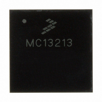
MC13213 Freescale Semiconductor, MC13213 Datasheet - Page 12

MC13213
Manufacturer Part Number
MC13213
Description
IC TXRX RF 2.4GHZ FLSH 60K 71LGA
Manufacturer
Freescale Semiconductor
Series
MC1321xr
Datasheet
1.1321XCSK-BDM.pdf
(70 pages)
Specifications of MC13213
Frequency
2.4GHz
Data Rate - Maximum
250kbps
Modulation Or Protocol
802.15.4 Zigbee
Applications
General Purpose
Power - Output
3dBm
Sensitivity
-92dBm
Voltage - Supply
1.8 V ~ 3.6 V
Current - Receiving
42mA
Current - Transmitting
35mA
Data Interface
PCB, Surface Mount
Memory Size
60kB Flash, 4kB RAM
Antenna Connector
PCB, Surface Mount
Operating Temperature
-40°C ~ 85°C
Package / Case
71-LGA
Number Of Receivers
1
Number Of Transmitters
1
Wireless Frequency
2.4 GHz to 2.48 GHz
Interface Type
SPI
Output Power
0 dBm to 2 dBm
Operating Supply Voltage
2 V to 3.4 V
Maximum Operating Temperature
+ 85 C
Mounting Style
SMD/SMT
Maximum Supply Current
42 mA
Minimum Operating Temperature
- 40 C
Protocol Supported
802.15.4
Lead Free Status / RoHS Status
Lead free / RoHS Compliant
Available stocks
Company
Part Number
Manufacturer
Quantity
Price
Company:
Part Number:
MC13213
Manufacturer:
FREESCALE Semiconductor
Quantity:
337
Part Number:
MC13213
Manufacturer:
FREESCALE
Quantity:
20 000
Company:
Part Number:
MC13213R2
Manufacturer:
BROADCOM
Quantity:
1
Part Number:
MC13213R2
Manufacturer:
FREESCALE
Quantity:
20 000
12
1
2
FLAG VSS
Pin #
The transceiver GPIO pins default to inputs at reset. There are no programmable pullups on these pins. Unused GPIO pins
should be tied to ground if left as inputs, or if left unconnected, they should be programmed as outputs set to the low state.
During low power modes, input must remain driven by MCU.
57
58
59
60
61
62
63
64
65
66
67
68
69
70
71
PTB5/AD1P5
PTB6/AD1P6
PTB7/AD1P7
VREFH
VREFL
PTA0/KBI1P0
PTA1/KBI1P1
PTA2/KBI1P2
PTE5/SPSCK1
PTE4/MOSI1
PTE3/MISO1
PTE2/SS1
IRQ
PTD1
PTD3
Pin Name
Input/Output
Input/Output
Input/Output
Input
Input
Digital
Input/Output
Digital
Input/Output
Digital
Input/Output
SPICLK
MOSI
MISO
CE
M_IRQ
RXTXEN
M_RST
Power input
Type
Table 2. Pin Function Description (continued)
MC13211/212/213 Technical Data, Rev. 1.8
Modem SPI slave MISO
MCU Port B Bit 5 / ATD
analog Channel 5
MCU Port B Bit 6 / ATD
analog Channel 6
MCU Port B Bit 7 / ATD
analog Channel 7
MCU high reference
voltage for ATD
MCU low reference voltage
for ATD
MCU Port A Bit 0 /
Keyboard Input Bit 0
MCU Port A Bit 1 /
Keyboard Input Bit 1
MCU Port A Bit 2 /
Keyboard Input Bit 2
MCU SPI master SPI clock
output drives modem
SPICLK slave clock input.
MCU SPI master MOSI
output drives modem slave
MOSI input
output drives MCU master
MISO input
MCU SPI master SS
output drives modem slave
CE input
Modem interrupt request
M_IRQ output drives MCU
IRQ input
MCU Port D Bit 1 drives
the RXTXEN input to the
modem to enable TX or RX
or CCA operations.
MCU Port D Bit 3 drives
the reset M_RST input to
the modem.
External package flag.
Common VSS
Description
Normally factory test. Do not connect
Normally factory test. Do not connect
Normally factory test. Do not connect
Normally factory test. Do not connect
Normally factory test. Do not connect
Normally factory test. Do not connect
Normally factory test. Do not connect
Connect to ground.
Functionality
Freescale Semiconductor


