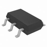
LTC4401-1ES6#TR Linear Technology, LTC4401-1ES6#TR Datasheet - Page 7

LTC4401-1ES6#TR
Manufacturer Part Number
LTC4401-1ES6#TR
Description
IC RF POWER CONTROLLER TSOT23-6
Manufacturer
Linear Technology
Datasheet
1.LTC4401-1ES6TR.pdf
(16 pages)
Specifications of LTC4401-1ES6#TR
Rf Type
Cellular, GSM, GPRS, PCS, Wireless Modem, TDMA
Frequency
300MHz ~ 2.7GHz
Features
Single Output
Package / Case
TSOT-23-6, TSOT-6
Lead Free Status / RoHS Status
Contains lead / RoHS non-compliant
Other names
LTC4401-1ES6TR
LTC44011ES6TR
LTC44011ES6TR
Available stocks
Company
Part Number
Manufacturer
Quantity
Price
APPLICATIONS
Operation
The LTC4401-X RF power control amplifier integrates
several functions to provide RF power control over fre-
quencies ranging from 300MHz to 2.7GHz. This product is
well suited to control RF power amplifiers that exhibit slow
turn-on times. The device also prevents damage to the RF
power amplifier due to overvoltage conditions. These
functions include an internally compensated power con-
trol amplifier to control the RF output power, an autozero
section to cancel internal and external voltage offsets, an
RF Schottky diode peak detector and amplifier to convert
the RF feedback signal to DC, a V
compression and a bandgap reference.
Band Selection
The LTC4401-2 is designed to drive two separate power
control lines. The BSEL pin will select V
V
being asserted high.
Control Amplifier
The control amplifier supplies the power control voltage to
the RF power amplifier. A portion (typically – 19dB for low
frequencies and –14dB for high frequencies) of the RF
output voltage is sampled, via a directional coupler, to
close the gain control loop. When a DAC voltage is applied
to PCTL, the amplifier quickly servos V
the detected feedback voltage applied to the RF pin matches
the voltage at PCTL. This feedback loop provides accurate
RF power control. V
current and 100pF load capacitor.
Control Amplifier Compression
The gain compression breakpoints are at PCTL = 80mV
and PCTL = 160mV. Above 160mV the gain does not
change. The compression changes the feedback attenua-
tion thereby reducing the loop gain.
RF Detector
The internal RF Schottky diode peak detector and ampli-
fier converts the RF feedback voltage from the directional
PCB
when high. BSEL must be established prior to SHDN
U
PCA/B
INFORMATION
is capable of driving a 6mA load
U
PCA/B
W
overvoltage clamp,
PCA/B
PCA
when low and
positive until
U
coupler to a low frequency voltage. This voltage is com-
pared to the DAC voltage at the PCTL pin by the control
amplifier to close the RF power control loop. The RF pin
input resistance is typically 250
range of this pin is 300MHz to 2700MHz for the LTC4401-1
and 300MHz to 2000MHz for the LTC4401-2. The detector
demonstrates excellent efficiency over a wide range of
input power. The Schottky detector is biased at about
60 A and drives an on-chip peak detector capacitor of
28pF.
Autozero
An autozero system is included to improve power pro-
gramming accuracy over temperature. This section can-
cels internal offsets associated with the Schottky diode
detector and control amplifier. External offsets associated
with the DAC driving the PCTL pin are also cancelled.
Offset drift due to temperature is cancelled between each
burst. The maximum offset voltage allowed at the DAC
output is limited to 400mV. Autozeroing is performed
during a 10 s period after SHDN is asserted high. An
internal timer enables the V
autozero capacitors are held and the V
nected to the control amplifier output. The hold droop
voltage of typically < 1 V/ms provides for accurate offset
cancellation. The part should be shut down between
bursts or after multiple consecutive bursts.
Filter
There is a 270kHz two pole filter included in the PCTL path
to remove DAC noise.
Protection Features
The RF power amplifier control voltage pin is overvoltage
protected. The V
V
attempts to exceed this voltage.
Modes of Operation
Shutdown: The part is in shutdown mode when SHDN is
low. V
is typically 10 A.
PCA/B
PCA/B
to 2.9V when the gain and PCTL input combination
is held at ground and the power supply current
LTC4401-1/LTC4401-2
PCA/B
overvoltage clamp regulates
PCA/B
output after 10 s. The
and the frequency
PCA/B
pin is con-
4401fa
7


