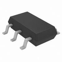
LTC4401-1ES6#TR Linear Technology, LTC4401-1ES6#TR Datasheet

LTC4401-1ES6#TR
Specifications of LTC4401-1ES6#TR
LTC44011ES6TR
Available stocks
Related parts for LTC4401-1ES6#TR
LTC4401-1ES6#TR Summary of contents
Page 1
... The shutdown feature disables the part and reduces the supply current to < dual control channel version (LTC4401-2) is also available in an 8-pin MSOP package. , LTC and LT are registered trademarks of Linear Technology Corporation. ...
Page 2
... SHDN = HI, unless otherwise noted 0mA VPCA (Note (Note 8) PCTL < 80mV LOAD PCTL > 160mV = 100pF, LOAD ORDER PART TOP VIEW NUMBER BSEL LTC4401-2EMS8 6 SHDN 5 PCTL MS8 PART MARKING MS8 PACKAGE = 250 C/W LTXC JA MIN TYP MAX 2 1.2 1 2.7 2.9 3 ...
Page 3
... Referenced to V Note 1: Absolute Maximum Ratings are those values beyond which the life of a device may be impaired. Note 2: The LTC4401-X is guaranteed to meet performance specifications from Specifications over the – operating temperature range are assured by design, characterization and correlation with statistical process controls. ...
Page 4
... A coupling capacitor of 33pF CC must be used to connect to the ground referenced direc- tional coupler. The frequency range is 300MHz to 2700MHz for the LTC4401-1 and 300MHz to 2000MHz for the LTC4401-2. This pin has an internal 250 termination, an internal Schottky diode detector and peak detector capaci- tor. ...
Page 5
... GND 2 V REF VBG Li-Ion AUTOZERO – GAIN – 80mV – 270kHz FILTER + 38k RF DET – V 22k REF 51k 33.4k TXENB 10 s DELAY 150k 4 3 PCTL SHDN LTC4401-1/LTC4401-2 50 TXENB + GM CLAMP + C BUFFER C – 30k 30k + – 100 CONTROL LTC4401-1 4401 PCA 4401fa 5 ...
Page 6
... TXENB AUTOZERO – – 80mV – 270kHz FILTER 38k V + 22k REF 51k – 33.4k 6k TXENB CONTROL 150k 5 7 PCTL BSEL RF PA 1.8GHz/1.9GHz + BUF A CLAMP + MUX1 MUX2 C C – 30k 30k 12 BUF B 100 12 V PCA 100 LTC4401 PCA 3 V PCB 4401-2 BD 4401fa ...
Page 7
... DAC voltage at the PCTL pin by the control amplifier to close the RF power control loop. The RF pin input resistance is typically 250 range of this pin is 300MHz to 2700MHz for the LTC4401-1 and 300MHz to 2000MHz for the LTC4401-2. The detector demonstrates excellent efficiency over a wide range of input power ...
Page 8
... V START PCTL T1: LTC4401-X COMES OUT OF SHUTDOWN 12 s PRIOR TO BURST T2: INTERNAL TIMER COMPLETES AUTOZERO CORRECTION, <10 s T3: BASEBAND CONTROLLER STARTS RF POWER RAMP AFTER SHDN IS ASSERTED HIGH T4: BASEBAND CONTROLLER COMPLETES RAMP UP T5: BASEBAND CONTROLLER STARTS RF POWER RAMP DOWN AT END OF BURST T6: LTC4401-X RETURNS TO SHUTDOWN MODE BETWEEN BURSTS ...
Page 9
... Loop voltage losses supplied by the directional coupler CODE will improve phase margin. The larger the directional coupler loss the more stable the loop will become. How- ever, larger losses reduce the RF signal to the LTC4401-X and detector performance may be degraded at low power levels. (See RF Detector Characteristics.) 4401 F01 ...
Page 10
... Gain peaking may occur, resulting in higher bandwidth and lower phase margin than predicted from the open-loop Bode plot. A low frequency AC SPICE model of the LTC4401-X power controller is included to better determine pole and zero interactions. The user can apply external gains and poles to determine bandwidth and phase margin ...
Page 11
... It should be remembered that models are a simplification of the actual circuit. CONTROLLED RF OUTPUT POWER 4401 F04 Figure 5. SPICE Model Open-Loop Gain and Phase Characteristics from LTC4401-1/LTC4401-2 80 180 LOAD 70 160 C = 33pF ...
Page 12
... VPCTLO, VRF, Adjust EFB gain to reflect external gain, currently set at 3X** *EFB RF 0 VPCA VIN 3 *VIN VIN *VPCTLO PCTL **Open-loop connections, comment-out EFB, VIN and VPCTLO****** VPCTLO PCTL VRF ******Add AC statement and print statement as required*** .AC DEC 50 100 1E7 *****for PSPICE only***** .OP .PROBE ************************* .END Figure 6. LTC4401-X Low Frequency AC SPICE Model 4401fa ...
Page 13
... LX1 1E-6 1E-6 CC1 65E-3 ND11 ND12 GX6 GXFB + + RX6 1E6 GM GM – – 1E-6 33E-6 CX6 1.2E-15 Figure 7. LTC4401-X Low Frequency AC Model LTC4401-1/LTC4401-2 ND6 ND7 GX3 GX4 + + RX2 RX3 1E6 GM 1E6 GM – – 1E-6 1E-6 CX2 CX3 8E-15 32E-15 ...
Page 14
... LTC4401-1/LTC4401-2 PACKAGE DESCRIPTIO 0.62 0.95 MAX REF 3.85 MAX 2.62 REF RECOMMENDED SOLDER PAD LAYOUT PER IPC CALCULATOR 0.20 BSC DATUM ‘A’ 0.30 – 0.50 REF NOTE: 1. DIMENSIONS ARE IN MILLIMETERS 2. DRAWING NOT TO SCALE 3. DIMENSIONS ARE INCLUSIVE OF PLATING 4. DIMENSIONS ARE EXCLUSIVE OF MOLD FLASH AND METAL BURR 5 ...
Page 15
... DETAIL “A” (.193 .006) 0 – 6 TYP 0.53 0.152 1.10 (.021 .006) (.043) DETAIL “A” MAX SEATING PLANE 0.22 – 0.38 (.009 – .015) TYP LTC4401-1/LTC4401-2 0.52 (.0205 REF 3.00 0.102 (.118 .004) (NOTE 0.86 (.034) REF 0.127 0.076 ( ...
Page 16
... Step-Down DC/DC Converter LTC3405 1.5MHz, 250mA ThinSOT Buck Converter LTC4400 RF Power Controller in ThinSOT LTC5505 RF Power Detector in ThinSOT Linear Technology Corporation 16 1630 McCarthy Blvd., Milpitas, CA 95035-7417 (408) 432-1900 FAX: (408) 434-0507 LTC4401-2 Dual Band Cellular Telephone Transmitter 33pF LTC4401 900MHz RF PA SHDN V PCA ...


