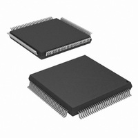
HSP50214BVIZ Intersil, HSP50214BVIZ Datasheet - Page 29

HSP50214BVIZ
Manufacturer Part Number
HSP50214BVIZ
Description
IC DOWNCONVERTER 14BIT 120-MQFP
Manufacturer
Intersil
Datasheet
1.HSP50214BVCZ.pdf
(62 pages)
Specifications of HSP50214BVIZ
Function
Downconverter
Rf Type
AMPS, CDMA, GSM, TDMA
Package / Case
120-MQFP, 120-PQFP
Lead Free Status / RoHS Status
Lead free / RoHS Compliant
Available stocks
Company
Part Number
Manufacturer
Quantity
Price
Company:
Part Number:
HSP50214BVIZ
Manufacturer:
HONGFA
Quantity:
30 000
Part Number:
HSP50214BVIZ
Manufacturer:
INTERSIL
Quantity:
20 000
The programmable parameters for the Timing NCO include
an Enable External Timing NCO Sync (Control Word 11, Bit
5), the serial word width, Number of Offset Frequency Bits
(Control Word 11, Bits 3-4), an Enable Offset Frequency
control (Control Word 11, Bit 2), a Clear NCO Accumulator
control (Control Word 11, Bit 1), a Timing NCO Phase
Accumulator Load On Update control (Control Word 11, Bit
0), the Timing NCO Center Frequency (Control Word 12), a
Timing Phase Offset (Control Word 13, Bits 0-7), a Timing
Frequency Strobe (Control Word 14) and a Timing Phase
Strobe (Control Word 15). Refer to the Carrier Synthesizer
Mixer Section for a detailed discussion of the serial interface
for the Timing NCO offset frequency word.
A timing error detector is provided for measuring the phase
difference between the timing NCO and a external clock input,
REFCLK. Timing Error is generated by comparing the values
of two programmable counters. One counter is clocked with
the Timing NCO carry out and the other is clocked by the
REFCLK. The 12-bit NCO Divide parameter is set in Control
Word 18, Bits 16-27. The NCO Divide parameter is the
preload to the counter that is clocked by the Timing NCO carry
out. The 12-bit Reference Divide parameter is set in Control
Word 18, Bits 0-11, and is the preload for the counter that is
clocked by the Reference clock. Figure 26 details the block
diagram of the timing error generation circuit. The 16-bits of
timing error are available both as a PDC serial output and as a
processor read parameter. See the Processor Read Section
for more details on accessing this value.
EN EXT TIMING NCO SYNC
†
NUMBER OF SOF BITS
SYNCIN2
TIMING PHASE STROBE
PHASE OFFSET
Controlled via microprocessor interface.
ENABLE SOF
TIMING NCO
SOFSYNC
FIGURE 26. TIMING NCO BLOCK DIAGRAM
SOF
†
†
ACCUMULATOR
SOF
SYNC
SHIFT REG
†
PHASE
32
†
SYNC
MUX
REG
†
0
TIMING NCO CENTER
29
FREQUENCY
8
32
REG
REG
REG
5
+
+
SCF
†
MUX
SYNC
CARRY OUT = RUN
FILTER STROBE
FILTER PHASE
SELECT
0
TIMING FREQ
STROBE
TIMING NCO
LOAD ON
UPDATE
PH ACC
CLEAR
PHASE
ACC
†
HSP50214B
†
†
†
Figure 27A illustrates an application where the Timing Error
Generator is used to lock the receiver samples with a
transmit data rate. In this example, the receive samples are
at four times the transmit data rate. An external loop filter is
required, whose frequency error output is fed into the Timing
NCO. This allows the loop to track out the long term drift
between the receive sample rate and the transmit data clock.
†
R
REFCLK
Tx DATA CLK
Controlled via microprocessor interface.
Controlled via microprocessor interface.
T
(REFCLK)
TIMING
= TOTAL DECIMATION (CIC, HB FILTERS AND FIR)
ACC.
NCO
TIMING
ACC.
NCO
FIGURE 27A. TIMING ERROR APPLICATION
FIGURE 27. TIMING ERROR GENERATION
PROGRAMMABLE
NCO DIVIDE = 4N
PROGRAMMABLE
PROGRAMMABLE
NCO DIVIDE
PROGRAMMABLE
DIVIDER
REFERENCE
DIVIDE = N
REFERENCE
CLKIN/R
DIVIDER
μP
DIVIDER
DIVIDE
DIVIDER
FILTER
LOOP
†
†
T
†
†
(NCO DIVIDE)/2
(NCO DIVIDE)/2
12
4
12
4
EN
EN
TO Tx BLOCK
(MODULATOR)
+
-
+
-
†
†
May 1, 2007
TE(15:0)
TE(15:0)
FN4450.4


