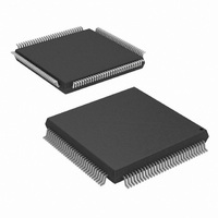
HSP50214BVCZ Intersil, HSP50214BVCZ Datasheet - Page 7

HSP50214BVCZ
Manufacturer Part Number
HSP50214BVCZ
Description
IC DOWNCONVERTER 14BIT 120-MQFP
Manufacturer
Intersil
Datasheet
1.HSP50214BVCZ.pdf
(62 pages)
Specifications of HSP50214BVCZ
Function
Downconverter
Rf Type
AMPS, CDMA, GSM, TDMA
Package / Case
120-MQFP, 120-PQFP
Lead Free Status / RoHS Status
Lead free / RoHS Compliant
Available stocks
Company
Part Number
Manufacturer
Quantity
Price
Company:
Part Number:
HSP50214BVCZ
Manufacturer:
AD
Quantity:
1 001
Functional Description
The HSP50214B Programmable Downconverter (PDC) is an
agile digital tuner designed to meet the requirements of a
wide variety of communications industry standards. The
PDC contains the processing functions needed to convert
sampled IF signals to baseband digital samples. These
functions include LO generation/mixing, decimation filtering,
programmable FIR shaping/bandlimiting filtering,
resampling, Automatic Gain Control (AGC), frequency
discrimination and detection as well as multi-chip
synchronization. The HSP50214B interfaces directly with a
DSP microprocessor to pass baseband and status data.
A top level functional block diagram of the HSP50214B is
shown in Figure 1. The diagram shows the major blocks and
multiplexers used to reconfigure the data path for various
architectures. The HSP50214B can be broken into 13
sections: Synchronization, Input, Input Level Detector,
Carrier Mixer/Numerically Control Oscillator (NCO), CIC
Decimating Filter, Halfband Decimating Filter, 255-Tap
Programmable FIR Filter, Automatic Gain Control (AGC),
Re-sampler/Halfband Filter, Timing NCO, Cartesian to Polar
Converter, Discriminator, and Output Sections. All of these
sections are configured through a microprocessor interface.
The HSP50214B has three clock inputs; two are required and
one is optional. The input level detector, carrier NCO, and CIC
decimating filter sections operate on the rising edge of the
input clock, CLKIN. The halfband filter, programmable FIR
filter, AGC, Re-Sampler / Halfband filters, timing NCO,
discriminator, and output sections operate on the rising edge
of PROCCLK. The third clock, REFCLK, is used to generate
timing error information.
NOTE: All of the clocks may be asynchronous.
PDC Applications Overview
This section highlights the motivation behind the key
programmable features from a communications system level
perspective. These motivations will be defined in terms of ability
to provide DSP processing capability for specific modulation
formats and communication applications. The versatility of the
Programmable Downconverter can be intimidating because of
the many Control Words required for chip configuration. This
section provides system level insight to help allay reservations
about this versatile DSP product. It should help the designer
capitalize on the greatest feature of the PDC - VERSATILITY
THROUGH PROGRAMMABILITY. It is this feature, when fully
understood, that brings the greatest return on design
investment by offering a single receiver design that can process
the many waveforms required in the communications
marketplace.
FDM Based Standards and Applications
Table 1 provides an overview of some common frequency
division multiplex (FDM) base station applications to which the
PDC can be applied. The PDC provides excellent selectivity
7
HSP50214B
for frequency division multiple access (FDMA) signals. This
high selectivity is achieved with 0.012Hz resolution frequency
control of the NCO and the sharp filter responses capable with
a 255-tap, 22-bit coefficient FIR filter. The 16-bit resolution out
of the Cartesian to Polar Coordinate Converter are routed to
the frequency detector, which is followed by a 63-tap, 22-bit
coefficient FIR filter structure for facilitating FM and FSK
detection. The 14-bit input resolution is the smallest bit
resolution found throughout the conversion and filtering
sections, providing excellent dynamic range in the DSP
processing. A unique input gain scaler adds an additional
42dB of range to the input level variation, to compensate for
changes in the analog RF front end receive equipment.
Synchronization circuitry allows precise timing control of the
base station reconfiguration for all receive channels
simultaneously. Portions of this table were corroborated with
reference [2].
TDM Based Standards and Applications
Table 2 provides an overview of some common Time Division
Multiplexed (TDM) base station applications to which the PDC
can be applied. For time division multiple access (TDMA)
applications, such as North American TDMA (IS136), where
30kHz is the received band of interest for the PCS
basestation, the PDC offers 0.012Hz frequency resolution in
downconversion in addition to α = 0.35 matched
(programmable) filtering capability. The π/4 DPSK modulation
can be processed using the PDC Cartesian to Polar
coordinate converter and dφ/dt detector circuitry or by
processing the I/Q samples in the DSP μP. The PDC provides
STANDARD
CHANNELS
DEVIATION
DEVIATION
# TRAFFIC
CONTROL
CONTROL
TABLE 1. CELLULAR PHONE BASE STATION
CHANNEL
CHANNEL
MODULA-
MODULA-
RX BAND
BW (kHz)
(Kbps)
VOICE
PEAK
PEAK
(MHz)
RATE
TION
(kHz)
(kHz)
TION
APPLICATIONS USING FDMA
824-849
(IS-91)
AMPS
FSK
832
FM
30
12
10
8
MCS-L1
MCS-L2
925-940
1200
25.0
12.5
FSK
600
FM
4.5
0.3
5
NMT-400
NMT-900
453-458
890-915
1999
12.5
FSK
200
FM
3.5
1.2
25
5
451-456
C450
20.0
10.0
FSK
222
444
FM
2.5
5.3
4
May 1, 2007
871-904
915-925
ETACS
NTACS
1240
25.0
12.5
FSK
FN4450.4
800
FM
9.5
6.4
8


