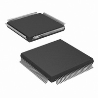
HSP50214BVCZ Intersil, HSP50214BVCZ Datasheet - Page 50

HSP50214BVCZ
Manufacturer Part Number
HSP50214BVCZ
Description
IC DOWNCONVERTER 14BIT 120-MQFP
Manufacturer
Intersil
Datasheet
1.HSP50214BVCZ.pdf
(62 pages)
Specifications of HSP50214BVCZ
Function
Downconverter
Rf Type
AMPS, CDMA, GSM, TDMA
Package / Case
120-MQFP, 120-PQFP
Lead Free Status / RoHS Status
Lead free / RoHS Compliant
Available stocks
Company
Part Number
Manufacturer
Quantity
Price
Company:
Part Number:
HSP50214BVCZ
Manufacturer:
AD
Quantity:
1 001
POSITION
POSITION
POSITION
POSITION
31-28
27-16
15-12
11-0
31-6
31-0
BIT
BIT
N/A
BIT
BIT
4-3
5
2
1
0
Reserved
Upper Limit
Reserved
Lower Limit
Sample AGC Gain
Level
Reserved
Enable External
Timing NCO Sync
Number of Offset
Frequency Bits
Enable Offset
Frequency
Clear Phase
Accumulator
Timing NCO Phase
Accumulator Load On
Update
Timing NCO Center
Frequency
CONTROL WORD 10: AGC SAMPLE GAIN CONTROL STROBE (SYNCHRONIZED TO PROCCLK)
FUNCTION
FUNCTION
FUNCTION
FUNCTION
CONTROL WORD 12: TIMING NCO CENTER FREQUENCY (SYNCHRONIZED TO PROCCLK)
CONTROL WORD 11: TIMING NCO CONFIGURATION (SYNCHRONIZED TO PROCCLK)
CONTROL WORD 9: AGC CONFIGURATION 2 (SYNCHRONIZED TO PROCCLK)
50
Reserved.
Maximum Gain/Minimum Signal. The upper four bits are used for exponent; the remaining bits form the
mantissa in the fractional offset binary: [eeeemmmmmmmm]. See the AGC Section for details. Bit 27 is
the MSB. The gain is in dB. G = (6.02)(eeee) + 20log
eeee = Floor [log
mmmmmmmm = Floor [256(10
Reserved.
Minimum Gain/Maximum Signal. The upper four bits are used for exponent; the remaining bits form the
mantissa in the fractional offset binary: [eeeemmmmmmmm]. See the AGC Section for details. Bit 11 is
the MSB. The gain is in dB. G = (6.02)(eeee) + 20log
eeee = Floor [log
mmmmmmmm = Floor [256(10
Writing to this location samples the output of the AGC loop filter to stabilize the value for μP reading.
Reserved.
0- SYNCIN2 has no effect on the timing NCO.
1- When SYNCIN2 is asserted, the timing NCO center frequency and phase are updated with the value
loaded in their holding registers. If bit 0 of this word is set to 1, the phase accumulator feedback is also
zeroed.
00 - 8 bits.
01 - 16.
10 - 24.
11 - 32.
0- Zero Offset Frequency to Adder.
1- Enable Offset Frequency.
0- Enable Accumulator.
1- Zero Feedback in Accumulator.
When this bit is set to 1, the μP update to the timing NCO frequency or an external timing NCO load
using SYNCIN2 will zero the feedback of the phase accumulator as well as update the phase and
frequency. This function can be used to set the NCO to a known phase synchronized to an external
event.
These bits control the frequency of the timing NCO. The frequency range of the NCO is from 0 to
F
the equation: N =(f
loading, a transfer to the Active Register is done by writing to Control Word 14 or by generating a
SYNCIN2 with Control Word 11, Bit 5 set to 1.
RESAMP
where F
2
2
(10
(10
RESAMP
OUT
HSP50214B
GAIN dB/20
GAIN dB/20
/ F
RESAMP
is the input sample rate to the resampling filter. The bits are computed by
GAIN dB/20
GAIN dB/20
)]
)]
)*2
32
. Bit 31 is the MSB. This location is a holding register. After
/2
/2
DESCRIPTION
DESCRIPTION
DESCRIPTION
DESCRIPTION
eeee
eeee
- 1)]
- 1)]
10
10
(1.0 + 0.mmmmmmmm)
(1.0 + 0.mmmmmmmm)
May 1, 2007
FN4450.4


