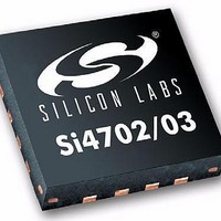
SI4703-B17-EVB Silicon Laboratories Inc, SI4703-B17-EVB Datasheet - Page 12

SI4703-B17-EVB
Manufacturer Part Number
SI4703-B17-EVB
Description
BOARD EVAL SI4703 VERSION B
Manufacturer
Silicon Laboratories Inc
Type
Tunerr
Datasheet
1.SI4703-B17-EVB.pdf
(46 pages)
Specifications of SI4703-B17-EVB
Frequency
76MHz ~ 108MHz
Lead Free Status / RoHS Status
Lead free / RoHS Compliant
For Use With/related Products
Si4703
Lead Free Status / RoHS Status
Lead free / RoHS Compliant, Lead free / RoHS Compliant
Si4702/03-C19
Table 8. FM Receiver Characteristics
(V
12
Parameter
Input Frequency
Sensitivity
Sensitivity (50 matching
network)
RDS Sensitivity
LNA Input Resistance
LNA Input Capacitance
Input IP3
AM Suppression
Adjacent Channel Selectivity
Alternate Channel Selectivity
Spurious Response Rejection
RCLK Frequency
RCLK Frequency Tolerance
Audio Output Voltage
Audio Output L/R Imbalance
Audio Frequency Response Low
Audio Frequency Response High
Audio Stereo Separation
Notes:
D
= V
1. Additional testing information is available in Application Note AN234. Volume = maximum for all tests.
2. Important Note: To ensure proper operation and FM receiver performance, follow the guidelines in “AN231:
3. F
4. MONO = 1, and L = R unless noted otherwise.
5. f = 22.5 kHz.
6. B
7. Typical sensitivity with headphone matching network.
8. Guaranteed by characterization.
9. V
10. |f
11. The channel spacing is selected with the SPACE[1:0] bits. Refer to "6. Register Descriptions" on page 23. Seek/Tune
12. f = 75 kHz.
13. The de-emphasis time constant is selected with the DE bit. Refer to "6. Register Descriptions" on page 23.
14. At LOUT and ROUT pins.
15. Do not enable STC interrupts before the powerup time is complete. If STC interrupts are enabled before the powerup
16. Minimum and maximum at room temperature (25 °C).
A
Si4700/01/02/03 Headphone and Antenna Interface.” Silicon Laboratories will evaluate schematics and layouts for
qualified customers.
timing is guaranteed for 100 and 200 kHz channel spacing.
time is complete, an interrupt will be generated within the powerup interval when the initial default tune operation is
complete. See "AN230: Si4700/01/02/03 Programmer’s Guide" for more information.
= 2.7 to 5.5 V, V
MOD
2
AF
EMF
3,4,5,6,8
8,10
– f
3,4,5,6,7
= 300 Hz to 15 kHz, A-weighted.
1
= 1 mV.
= 1 kHz, 75
| > 1 MHz,
8
3,4,5,8,9
3,4,5,9
8,9
f
IO
0
µ
8,9
= 2 x f
s de-emphasis
= 1.5 to 3.6 V, T
3,9,12
11
3,4,9,12
8
1
– f
8
8
2
. AGC
Symbol
A
f
= –20 to 85 °C)
RF
is disabled by setting AGCD = 1. Refer to "6. Register Descriptions" on page 23.
1,2
Frequency Spacing =
Frequency Spacing =
RDS BLER < 5%
(S+N)/N = 26 dB
(S+N)/N = 26 dB
Rev. 1.1
Test Condition
100 or 200 kHz
f = 2 kHz,
±200 kHz
±400 kHz
In-band
m = 0.3
50 kHz
–3 dB
–3 dB
–200
Min
104
–50
76
40
35
60
35
72
15
25
—
—
—
—
—
—
3
4
32.768
Typ
106
1.7
1.1
15
55
50
70
80
—
—
—
—
—
—
—
—
4
5
Max
108
200
3.5
50
90
30
—
—
—
—
—
—
—
—
—
—
5
6
1
dBµVEMF
µVEMF
µVEMF
µVEMF
mV
MHz
Unit
ppm
kHz
kHz
k
pF
dB
dB
dB
dB
dB
Hz
dB
RMS


