RF5110GPCK-410 RFMD, RF5110GPCK-410 Datasheet - Page 4
RF5110GPCK-410
Manufacturer Part Number
RF5110GPCK-410
Description
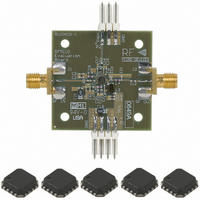
KIT EVAL FOR RF5110G
Manufacturer
RFMD
Type
Amplifierr
Datasheet
1.RF5110GTR7.pdf
(22 pages)
Specifications of RF5110GPCK-410
Frequency
800MHz ~ 950MHz
For Use With/related Products
RF5110G
Lead Free Status / RoHS Status
Lead free / RoHS Compliant
Other names
689-1054
RF5110GPCBA-410
RF5110GPCBA-410
Available stocks
Company
Part Number
Manufacturer
Quantity
Price
Company:

Part Number:
RF5110GPCK-410
Manufacturer:
RFMD
Quantity:
5 000


RF5110G
4 of 22
Base
Pkg
Pin
10
11
12
13
14
15
16
1
2
3
4
5
6
7
8
9
Function
RF OUT
RF OUT
RF OUT
RF OUT
GND1
GND2
APC2
APC1
VCC1
RF IN
VCC2
VCC2
GND
2F0
VCC
NC
NC
Description
Power supply for the pre-amplifier stage and interstage matching. This pin
forms the shunt inductance needed for proper tuning of the interstage
match. Refer to the application schematic for proper configuration. Note
that position and value of the components are important.
Ground connection for the pre-amplifier stage. Keep traces physically short
and connect immediately to the ground plane for best performance. It is
important for stability that this pin has it’s own vias to the groundplane, to
minimize any common inductance.
RF Input. This is a 50Ω input, but the actual impedance depends on the
interstage matching network connected to pin 1. An external DC blocking
capacitor is required if this port is connected to a DC path to ground or a
DC voltage.
Ground connection for the driver stage. To minimize the noise power at the
output, it is recommended to connect this pin with a trace of about 40mil
to the ground plane. This will slightly reduce the small signal gain, and
lower the noise power. It is important for stability that this pin have it’s own
vias to the ground plane, minimizing common inductance.
Power supply for the driver stage and interstage matching. This pin forms
the shunt inductance needed for proper tuning of the interstage match.
Please refer to the application schematic for proper configuration, and
note that position and value of the components are important.
Same as pin 5.
Not connected.
Connection for the second harmonic trap. This pin is internally connected
to the RF OUT pins. The bonding wire together with an external capacitor
form a series resonator that should be tuned to the second harmonic fre-
quency in order to increase efficiency and reduce spurious outputs.
RF Output and power supply for the output stage. Bias voltage for the final
stage is provided through this wide output pin. An external matching net-
work is required to provide the optimum load impedance.
Same as pin 9.
Same as pin 9.
Same as pin 9.
Not connected.
Power supply for the bias circuits.
Power Control for the output stage. See pin 16 for more details.
Power Control for the driver stage and pre-amplifier. When this pin is "low,"
all circuits are shut off. A "low" is typically 0.5V or less at room tempera-
ture. A shunt bypass capacitor is required. During normal operation this pin
is the power control. Control range varies from about 1.0V for -10dBm to
2.6V for +35dBm RF output power. The maximum power that can be
achieved depends on the actual output matching; see the application infor-
mation for more details. The maximum current into this pin is 5mA when
V
Ground connection for the output stage. This pad should be connected to
the ground plane by vias directly under the device. A short path is required
to obtain optimum performance, as well as to provide a good thermal path
to the PCB for maximum heat dissipation.
APC1
7628 Thorndike Road, Greensboro, NC 27409-9421 · For sales or technical
support, contact RFMD at (+1) 336-678-5570 or sales-support@rfmd.com.
=2.6V, and 0mA when V
APC
=0V.
Interface Schematic
See pin 3.
See pin 1.
See pin 3.
Same as pin 9.
Same as pin 9.
Same as pin 9.
See pin 16.
G N D
A P C
RF IN
From Bias
Stages
From Bias
Stages
From Bias
Stages
V C C
G N D
PCKG BASE
Rev A4 DS071026
RF OUT
VCC2
GND2
VCC1
GND
GND1
T o R F
S ta g e s
Related parts for RF5110GPCK-410
Image
Part Number
Description
Manufacturer
Datasheet
Request
R

Part Number:
Description:
3V GSM POWER AMPLIFIER
Manufacturer:
RF Micro Devices
Datasheet:

Part Number:
Description:
IC AMP HBT GAAS CATV 8-SOIC
Manufacturer:
RFMD
Datasheet:

Part Number:
Description:
IC AMP MMIC GAAS 12GHZ 4-MICROX
Manufacturer:
RFMD
Datasheet:

Part Number:
Description:
IC AMP 3V LOW-NOISE SOT23-6
Manufacturer:
RFMD
Datasheet:

Part Number:
Description:
KIT EVAL FOR NBB-310
Manufacturer:
RFMD
Datasheet:
Part Number:
Description:
IC AMPLIFIER MMIC LNA 8-QFN
Manufacturer:
RFMD
Datasheet:
Part Number:
Description:
IC AMP MMIC GAAS 4GHZ 4-MICROX
Manufacturer:
RFMD
Datasheet:
Part Number:
Description:
IC SWITCH 10W PHEMT SPDT 12QFN
Manufacturer:
RFMD
Datasheet:
Part Number:
Description:
IC QUADRATURE MODULATOR 16-SOIC
Manufacturer:
RFMD
Datasheet:
Part Number:
Description:
100MHZ TO 4000MHZ, GAAS PHEMT MMIC LOW NOISE AMPLIFIERS
Manufacturer:
RFMD
Part Number:
Description:
KIT EVAL FOR RF2336
Manufacturer:
RFMD
Datasheet:


Part Number:
Description:
IC AMP WLAN/LNA DVR 3V SOT23-5
Manufacturer:
RFMD
Datasheet:

Part Number:
Description:
IC AMP HBT GAAS LNA BYPASS 8-QFN
Manufacturer:
RFMD
Datasheet: