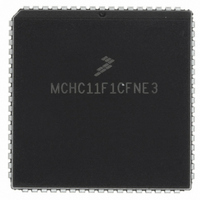
MCHC11F1CFNE3 Freescale Semiconductor, MCHC11F1CFNE3 Datasheet - Page 90

MCHC11F1CFNE3
Manufacturer Part Number
MCHC11F1CFNE3
Description
IC MCU 8BIT 1K RAM 68-PLCC
Manufacturer
Freescale Semiconductor
Series
HC11r
Specifications of MCHC11F1CFNE3
Core Processor
HC11
Core Size
8-Bit
Speed
3MHz
Connectivity
SCI, SPI
Peripherals
POR, WDT
Number Of I /o
30
Program Memory Type
ROMless
Eeprom Size
512 x 8
Ram Size
1K x 8
Voltage - Supply (vcc/vdd)
4.75 V ~ 5.25 V
Data Converters
A/D 8x8b
Oscillator Type
Internal
Operating Temperature
-40°C ~ 85°C
Package / Case
68-PLCC
A/d Inputs
8-Channel, 8-Bit
Eeprom Memory
512 Bytes
Input Output
30
Interface
SCI/SPI
Memory Type
EPROM
Number Of Bits
8
Package Type
68-pin PLCC
Programmable Memory
0 Bytes
Timers
3-16-bit
Voltage, Range
3-5.5 V
Controller Family/series
68HC11
No. Of I/o's
30
Eeprom Memory Size
512Byte
Ram Memory Size
1KB
Cpu Speed
3MHz
No. Of Timers
1
Embedded Interface Type
SCI, SPI
Rohs Compliant
Yes
Processor Series
HC11F
Core
HC11
Data Bus Width
8 bit
Program Memory Size
512 B
Data Ram Size
1 KB
Interface Type
SCI, SPI
Maximum Clock Frequency
3 MHz
Number Of Timers
1
Maximum Operating Temperature
+ 85 C
Mounting Style
SMD/SMT
Minimum Operating Temperature
- 40 C
On-chip Adc
8 bit, 8 Channel
Lead Free Status / RoHS Status
Lead free / RoHS Compliant
Program Memory Size
-
Lead Free Status / Rohs Status
RoHS Compliant part
Available stocks
Company
Part Number
Manufacturer
Quantity
Price
Company:
Part Number:
MCHC11F1CFNE3
Manufacturer:
FREESCALE
Quantity:
5 530
Company:
Part Number:
MCHC11F1CFNE3
Manufacturer:
FREESCALE
Quantity:
5 530
Company:
Part Number:
MCHC11F1CFNE3
Manufacturer:
Freescale Semiconductor
Quantity:
10 000
Company:
Part Number:
MCHC11F1CFNE3R
Manufacturer:
Freescale Semiconductor
Quantity:
10 000
7.4 Wakeup Feature
7.4.1 Idle-Line Wakeup
7.4.2 Address-Mark Wakeup
7-4
The wakeup feature reduces SCI service overhead in multiple receiver systems. Soft-
ware for each receiver evaluates the first character of each message. The receiver is
placed in wakeup mode by writing a one to the RWU bit in the SCCR2 register. While
RWU is one, all of the receiver-related status flags (RDRF, IDLE, OR, NF, and FE) are
inhibited (cannot become set). Although RWU can be cleared by a software write to
SCCR2, to do so would be unusual. Normally RWU is set by software and is cleared
automatically with hardware. Whenever a new message begins, logic alerts the sleep-
ing receivers to wake up and evaluate the initial character of the new message.
Two methods of wakeup are available: idle-line wakeup and address-mark wakeup.
During idle-line wakeup, a sleeping receiver awakens as soon as the RxD line be-
comes idle. In the address-mark wakeup, logic one in the most significant bit (MSB) of
a character wakes up all sleeping receivers.
To use the receiver wakeup method, establish a software addressing scheme to allow
the transmitting devices to direct a message to individual receivers or to groups of re-
ceivers. This addressing scheme can take any form as long as all transmitting and re-
ceiving devices are programmed to understand the same scheme. Because the
addressing information is usually the first frame(s) in a message, receivers that are not
part of the current task do not become burdened with the entire set of addressing
frames. All receivers are awake (RWU = 0) when each message begins. As soon as
a receiver determines that the message is not intended for it, software sets the RWU
bit (RWU = 1), which inhibits further flag setting until the RxD line goes idle at the end
of the message. As soon as an idle line is detected by receiver logic, hardware auto-
matically clears the RWU bit so that the first frame of the next message can be re-
ceived. This type of receiver wakeup requires a minimum of one idle-line frame time
between messages, and no idle time between frames in a message.
The serial characters in this type of wakeup consist of seven (eight if M = 1) information
bits and an MSB, which indicates an address character (when set to one, or mark).
The first character of each message is an addressing character (MSB = 1). All receiv-
ers in the system evaluate this character to determine if the remainder of the message
is directed toward this particular receiver. As soon as a receiver determines that a
message is not intended for it, the receiver activates the RWU function by using a soft-
ware write to set the RWU bit. Because setting RWU inhibits receiver-related flags,
there is no further software overhead for the rest of this message.
When the next message begins, its first character has its MSB set, which automatically
clears the RWU bit and enables normal character reception. The first character whose
MSB is set is also the first character to be received after wakeup because RWU gets
cleared before the stop bit for that frame is serially received. This type of wakeup al-
lows messages to include gaps of idle time, unlike the idle-line method, but there is a
loss of efficiency because of the extra bit time for each character (address bit) required
for all characters.
Freescale Semiconductor, Inc.
For More Information On This Product,
SERIAL COMMUNICATIONS INTERFACE
Go to: www.freescale.com
TECHNICAL DATA
MC68HC11F1


